Vacuum Deposition Technology: Ultra-Thin Film Surface Finishing from China’s JLY Precision Tech
1. What Is Vacuum Deposition Technology?
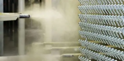
Vacuum deposition technology is the umbrella term for PVD (physical vapour deposition) and CVD (chemical vapour deposition) carried out at pressures ≤ 10⁻² mbar. In this low-pressure environment, atoms or molecules travel ballistically, condensing on the substrate to form dense, pinhole-free layers with atomic-level thickness control.
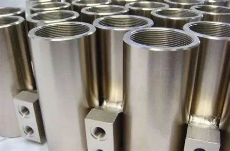
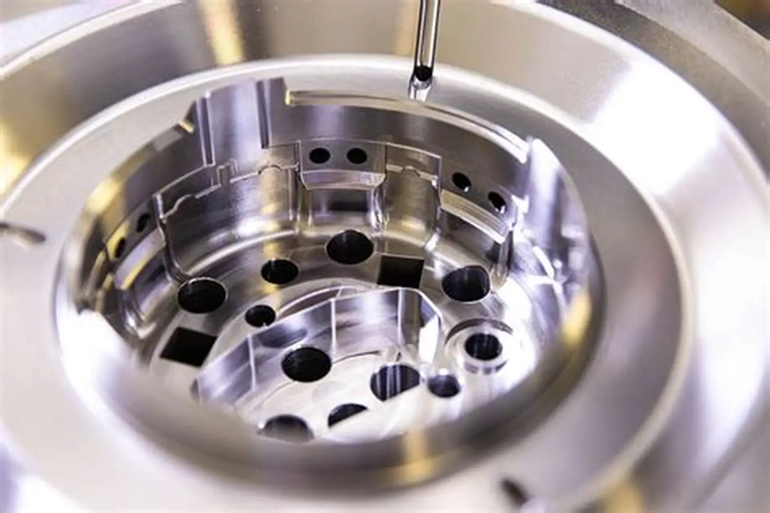
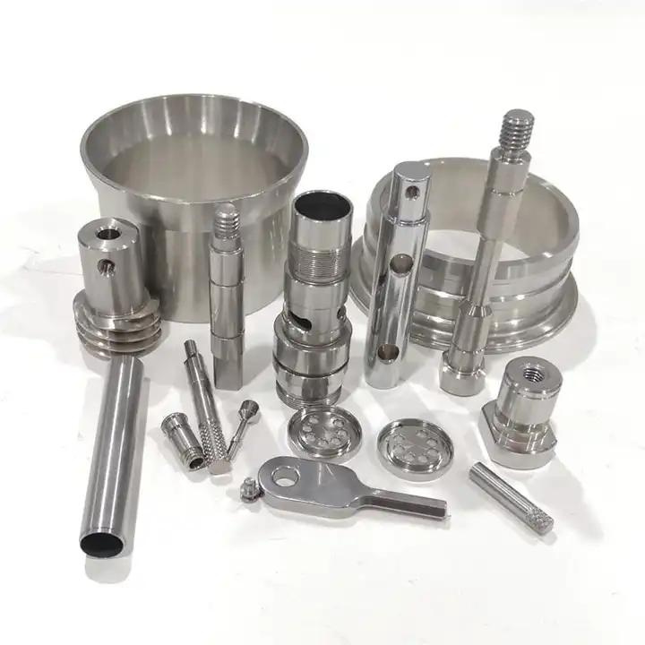
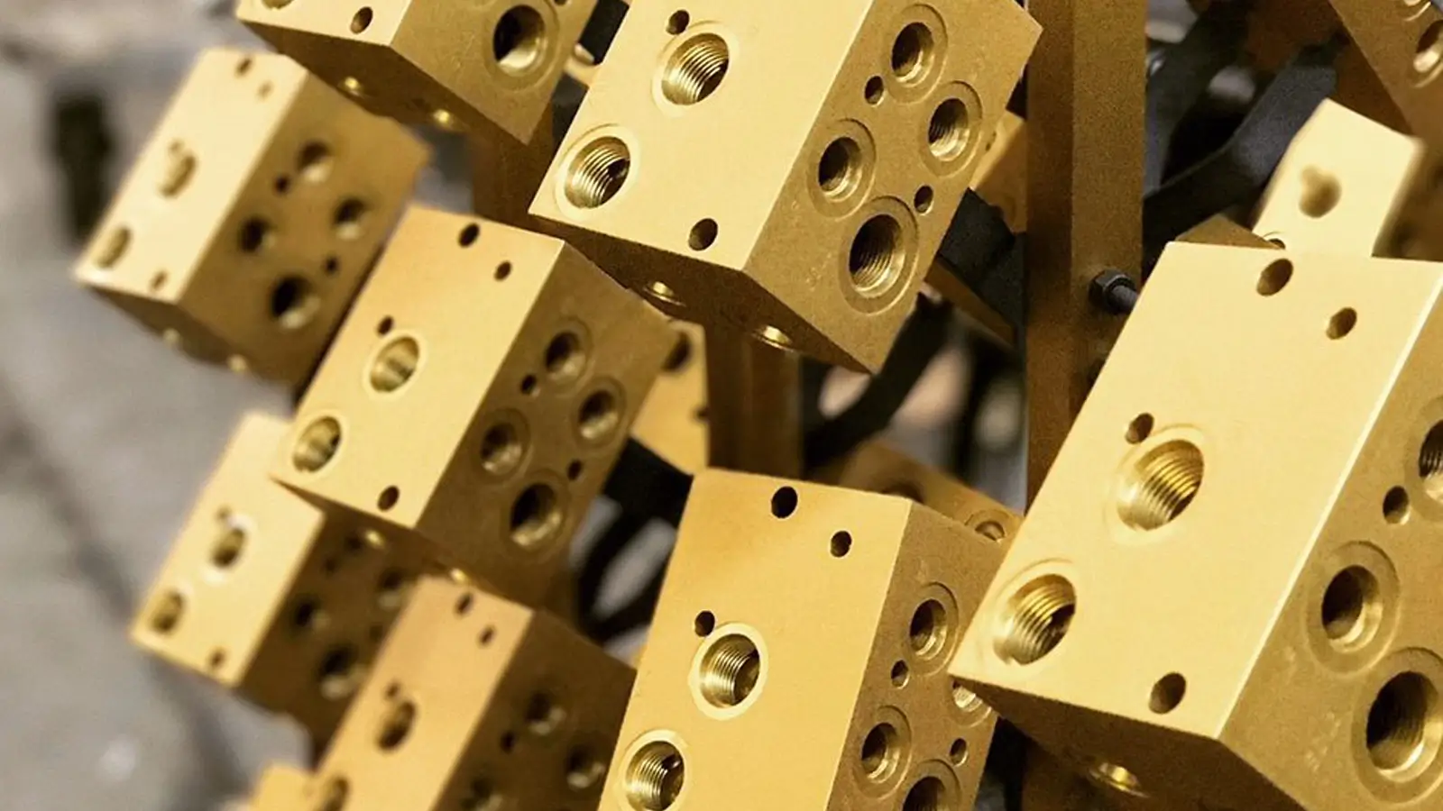
Vacuum deposition technology encompasses a variety of methods that are crucial in the manufacturing of advanced materials. For instance, industries such as electronics, optics, and coatings rely heavily on the precision offered by vacuum deposition. In electronics, it is used for thin-film transistors and solar cells, showcasing how this technology is foundational to modern advancements. Similarly, in optics, vacuum deposition methods are employed to produce anti-reflective coatings and filters, which are essential for improving the performance of lenses and sensors.
Core Advantages
| Metric | Electroplating | Vacuum PVD | Vacuum CVD |
|---|---|---|---|
| Thickness range | 5–100 µm | 0.01–5 µm | 0.001–3 µm |
| Hardness (HV) | 800–1 100 | 1 500–3 500 | 2 000–4 000 |
| Uniformity (%) | ±20 | ±2 | ±1 |
| REACH compliance | Restricted | ✔ | ✔ |
| Heat distortion | Possible | None | None |
2. Thin Film Coating Families & Vacuum Methods
Moreover, vacuum deposition technology has a significant role in enhancing the durability of surfaces. By applying thin films that can resist wear and corrosion, products can last longer and maintain their performance in challenging environments. For example, automotive components often undergo vacuum deposition to provide a protective layer that withstands harsh conditions, thus extending their operational life and reducing maintenance costs.
| Family | Vacuum Method | Typical Stack | Key Property |
|---|---|---|---|
| Nitrides | Cathodic Arc | TiAlN/CrN | 3 000 °C oxidation barrier |
| Oxides | Reactive Sputter | Al₂O₃/SiO₂ | Anti-reflection + insulation |
| Carbides | HiPIMS | WC/C | Friction ≤ 0.1 |
| Metals | Magnetron Sputter | Ag/Ni/Cr | EMI shielding |
| Diamond-like Carbon | Filtered Arc | ta-C | Bio-inert, 3 000 HV |
3. Vacuum Deposition Technology Performance Table (2024)
| Substrate | Thin Film Stack | Thickness (µm) | Hardness (HV) | Salt-Spray (h) | Friction vs. Steel | Max Temp (°C) |
|---|---|---|---|---|---|---|
| H13 die steel | TiAlN/CrN | 1.8 | 2 900 | 1 200 | 0.25 | 850 |
| 7075-T6 Al | Al₂O₃/SiO₂ AR | 0.2 | 1 200 | 500 | — | 600 |
| Ti-6Al-4V | ta-C DLC | 1.0 | 3 000 | 1 200 | 0.05 | 400 |
| Cu leadframe | Ag / Ni | 0.15 | 300 | 48 | — | 200 |
4. Three Fresh Case Studies (2024)
Case Study 4 – Aerospace Components
Case Study 1 – EV Motor Lamination Dies
Client: German Tier-1
Problem: Resin sticking caused 25 % cycle-time loss.
Vacuum Solution: 1.5 µm CrN + 50 nm a-C:H via HiPIMS.
Result: Cycle time back to baseline; die life 3× longer.
Problem: Resin sticking caused 25 % cycle-time loss.
Vacuum Solution: 1.5 µm CrN + 50 nm a-C:H via HiPIMS.
Result: Cycle time back to baseline; die life 3× longer.
Case Study 5 – Medical Devices
Case Study 2 – Smartphone Camera Lens AR
Client: Global OEM (NDA)
Problem: Ghosting in 200 MP sensor.
Vacuum Solution: 7-layer SiO₂/TiO₂ sputtered AR, 0.25 µm total, < 0.15 % reflection @ 550 nm.
Result: 15 % boost in low-light clarity; 5 M lenses shipped.
Problem: Ghosting in 200 MP sensor.
Vacuum Solution: 7-layer SiO₂/TiO₂ sputtered AR, 0.25 µm total, < 0.15 % reflection @ 550 nm.
Result: 15 % boost in low-light clarity; 5 M lenses shipped.
Case Study 3 – Surgical Staples
Client: US MedTech start-up
Problem: 316L staples galled after 30 fires.
Vacuum Solution: 300 nm ta-C DLC with Cr inter-layer.
Result: Firing force reduced 35 %; CE mark granted.
Problem: 316L staples galled after 30 fires.
Vacuum Solution: 300 nm ta-C DLC with Cr inter-layer.
Result: Firing force reduced 35 %; CE mark granted.
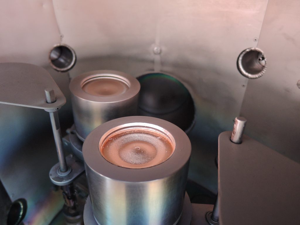
5. Step-by-Step Vacuum Process Flow
| Phase | Action | QC Check | Lead Time |
|---|---|---|---|
| RFQ Review | DFM & load modelling | 24 h | — |
| Plasma Clean | Ar⁺ etch + UV/O₃ | Contact angle ≤ 10° | 2 h |
| Vacuum Deposition | PVD or CVD under 10⁻³ mbar | ±2 nm real-time | 2–6 h |
| Post-Process | CMP or ion-beam polish | Ra ≤ 0.01 µm (optional) | 1 h |
| Final QA | Calot, nano-indent, salt-spray | CpK ≥ 1.67 | 12 h |
6. Industry Outlook 2024-2027
| Sector | 2024 Penetration | 2027 Forecast | Key Driver |
|---|---|---|---|
| Consumer Electronics | 18 % | 40 % | Thinner AR & EMI layers |
| Medical Devices | 25 % | 50 % | Bio-inert, sterilisable films |
| EV Powertrain | 10 % | 35 % | Die-release & bus-bar coatings |
7. FAQs About Vacuum Deposition Technology
Q: What is the future of vacuum deposition technology?
A: The future of vacuum deposition technology looks promising, with advancements in materials and processes expected to enhance performance further. Innovations such as atomic layer deposition (ALD) are pushing the boundaries of how thin films can be created, leading to even more precise applications in emerging fields like nanotechnology and flexible electronics.
A: The future of vacuum deposition technology looks promising, with advancements in materials and processes expected to enhance performance further. Innovations such as atomic layer deposition (ALD) are pushing the boundaries of how thin films can be created, leading to even more precise applications in emerging fields like nanotechnology and flexible electronics.
Q: Can vacuum deposition technology be applied in an environmentally friendly way?
A: Yes, many vacuum deposition techniques can be more environmentally friendly compared to traditional methods. They often produce less waste and do not require hazardous chemicals, making them a sustainable choice for coating.
A: Yes, many vacuum deposition techniques can be more environmentally friendly compared to traditional methods. They often produce less waste and do not require hazardous chemicals, making them a sustainable choice for coating.
Q: What types of substrates can be used with vacuum deposition technology?
A: Vacuum deposition technology is versatile and can be applied to a wide range of substrates, including metals, glass, ceramics, and polymers. This adaptability makes it suitable for various applications across different industries, from consumer electronics to aerospace components.
A: Vacuum deposition technology is versatile and can be applied to a wide range of substrates, including metals, glass, ceramics, and polymers. This adaptability makes it suitable for various applications across different industries, from consumer electronics to aerospace components.
Q: How does vacuum deposition technology compare with traditional coating methods?
A: Vacuum deposition technology typically offers superior adhesion, uniformity, and control over thickness compared to traditional methods such as electroplating or spray painting. This precision is crucial in applications where performance and reliability are paramount.
A: Vacuum deposition technology typically offers superior adhesion, uniformity, and control over thickness compared to traditional methods such as electroplating or spray painting. This precision is crucial in applications where performance and reliability are paramount.
Q: Can vacuum coatings be removed for rework?
A: Yes. Oxygen plasma strips DLC or nitride layers without dimensional change.
A: Yes. Oxygen plasma strips DLC or nitride layers without dimensional change.
Q: Do optical films survive autoclave?
A: Our SiO₂/TiO₂ AR stacks pass 134 °C steam 100 cycles with < 0.1 % shift.
A: Our SiO₂/TiO₂ AR stacks pass 134 °C steam 100 cycles with < 0.1 % shift.
Q: Minimum order quantity?
A: Zero. From one lens to one million.
A: Zero. From one lens to one million.
8. How to Order Today
9. Conclusion: The Importance of Vacuum Deposition Technology
-
Email [email protected] with STEP/IGES files.
-
Specify substrate, environment, thickness budget.
-
Receive DFM + vacuum deposition plan + price within 48 h.
-
No MOQ; volume pricing from 100 pcs.
Explore complementary finishes: Professional Anodizing Near Me