The Precision Art of Vacuum Metallizing: Advanced Surface Engineering for High-Performance Components
Introduction: The Evolution of Precision Surface Enhancement Technology
In the realm of advanced manufacturing where surface properties determine functional performance, vacuum metallizing represents a sophisticated surface engineering technology that transforms component capabilities at the atomic level. This precise deposition process, conducted in controlled vacuum environments, applies micron-thin metallic layers to substrates with exceptional uniformity and adhesion properties. At JLYPT, we’ve integrated specialized vacuum metallizing capabilities into our precision manufacturing ecosystem, creating components that achieve previously unattainable combinations of electrical conductivity, corrosion resistance, thermal management, and aesthetic refinement.
The distinction between conventional plating and vacuum metallizing manifests in measurable performance differentials: vacuum-deposited aluminum layers with 99.99% purity achieve surface resistivity of <0.1 Ω/□ compared to 2-5 Ω/□ for electroplated equivalents; vacuum-applied barrier coatings demonstrate pinhole densities of <0.1/cm² versus 5-20/cm² for wet processes; and decorative finishes maintain color consistency with ΔE<1.0 across production batches where traditional methods show ΔE>3.0 variations. Unlike electroplating processes that introduce hydrogen embrittlement risks or chemical baths with environmental concerns, vacuum metallizing utilizes clean physical deposition mechanisms that preserve substrate integrity while creating metallurgical bonds at the interface.
This comprehensive examination explores the scientific principles, technological implementations, and industrial applications of modern vacuum metallizing. We’ll analyze the vacuum physics governing deposition uniformity, the material science behind coating-substrate interactions, and the precision engineering required to metallize complex CNC-machined geometries. Whether you’re developing aerospace components requiring controlled emissivity coatings, medical devices needing biocompatible conductive surfaces, or consumer products demanding durable decorative finishes, understanding vacuum metallizing capabilities represents a critical dimension in component engineering. Discover how our integrated approach at JLYPT PVD Coating Services combines precision machining with advanced vacuum metallizing to create components with engineered surface properties.
The Physics of Vacuum Deposition: Principles and Mechanisms
Vacuum metallizing encompasses several physical deposition techniques that share fundamental operating principles but differ in their methods of material vaporization and transport. Understanding these mechanisms is essential for selecting the optimal process for specific applications.
Vacuum Environment Fundamentals
All vacuum metallizing processes operate within controlled vacuum chambers with pressure typically ranging from 10⁻² to 10⁻⁶ Torr (1.3 × 10⁻² to 1.3 × 10⁻⁶ Pa). This environment serves critical functions:
-
Mean Free Path Extension: Reducing atmospheric particle density allows vaporized coating atoms to travel directly from source to substrate without gas phase collisions, enabling line-of-sight deposition and precise thickness control.
-
Contamination Elimination: Removing oxygen, water vapor, and other reactive gases prevents oxide formation during deposition and ensures pure metallic or compound layer formation.
-
Plasma Generation Support: The low-pressure environment facilitates efficient creation and maintenance of plasma for enhanced deposition processes.
Thermal Evaporation Deposition
This foundational vacuum metallizing technique utilizes resistive or electron beam heating to vaporize source material:
-
Resistive Evaporation: Tungsten, molybdenum, or tantalum filaments or boats are resistively heated to temperatures exceeding the source material’s evaporation point (typically 1000-2000°C for common metals). The vaporized atoms travel ballistically to condense on substrates.
-
Electron Beam Evaporation: A focused electron beam with energy 5-40 keV is directed at the source material in a water-cooled copper crucible, creating localized heating and vaporization without contaminating the melt.
-
Deposition Characteristics: Thermal evaporation produces relatively low-energy particles (0.1-0.5 eV) with line-of-sight deposition patterns. The process achieves high deposition rates (1-10 nm/s) but limited throwing power for complex geometries.
Sputter Deposition Physics
Sputtering utilizes momentum transfer from energized plasma ions to dislodge atoms from a target material:
-
Direct Current (DC) Magnetron Sputtering: An argon plasma is established between a cathode (target) and anode (substrate/chamber). Ar⁺ ions accelerated by the electric field strike the target, physically ejecting atoms that deposit on substrates. Magnetic fields confine electrons near the target surface, increasing ionization efficiency.
-
Radio Frequency (RF) Sputtering: For insulating target materials, RF power at 13.56 MHz alternately charges the target as cathode and anode, preventing charge accumulation while maintaining plasma.
-
High Power Impulse Magnetron Sputtering (HiPIMS): Delivers extremely high power densities in short pulses (typically 50-200 µs at 0.1-10 kHz), generating highly ionized plasma (70-90%) with enhanced ionization compared to conventional DC sputtering (typically <10%).
Molecular Beam Epitaxy (MBE)
An ultra-high vacuum technique (10⁻⁸ to 10⁻¹² Torr) producing extremely pure, precisely controlled thin films with atomic-layer accuracy:
-
Effusion Cells: Thermally evaporate source materials with precise temperature control (±0.1°C)
-
In-situ Monitoring: Reflection high-energy electron diffraction (RHEED) provides real-time growth monitoring
-
Applications: Semiconductor devices, quantum structures, and research-grade coatings where purity and interface control are paramount
Table 1: Vacuum Metallizing Technology Comparison
| Process Parameter | Thermal Evaporation | DC Magnetron Sputtering | HiPIMS | Molecular Beam Epitaxy |
|---|---|---|---|---|
| Operating Pressure | 10⁻⁵ – 10⁻⁷ Torr | 1-10 mTorr | 1-10 mTorr | 10⁻⁸ – 10⁻¹² Torr |
| Particle Energy | 0.1-0.5 eV | 1-10 eV | 10-100 eV | 0.1-0.5 eV |
| Deposition Rate | 1-10 nm/s | 0.1-5 nm/s | 0.5-5 nm/s | 0.01-1 nm/s |
| Film Density | 85-95% theoretical | 95-99% theoretical | >99% theoretical | 99.9+% theoretical |
| Throwing Power | Poor (line-of-sight) | Good (some gas scattering) | Excellent (plasma guidance) | Excellent (ultra-high vacuum) |
| Ionization Rate | <1% | 5-10% | 70-90% | <1% |
| Optimal Applications | Reflective coatings, simple geometries | Conductive layers, complex shapes | Dense coatings, excellent adhesion | Semiconductor, quantum, research |
Material Systems for Vacuum Metallizing
The selection of deposition materials determines the functional properties imparted to components through vacuum metallizing.
Pure Metals and Alloys
-
Aluminum (Al): The most commonly vacuum-metallized material due to its excellent reflectivity (88-92% in visible spectrum), low cost, and good conductivity. Typically applied in thicknesses of 50-100 nm for decorative applications and 100-500 nm for functional coatings.
-
Copper (Cu): Exceptional electrical conductivity (1.68 × 10⁻⁸ Ω·m) makes it ideal for EMI/RFI shielding and conductive traces. Requires adhesion layers (typically chromium or nickel) on many substrates.
-
Chromium (Cr): Excellent adhesion promoter and corrosion-resistant underlayer. Often used in thicknesses of 10-50 nm as an interface between substrate and decorative or functional layers.
-
Gold (Au): Superior corrosion resistance, electrical conductivity, and aesthetic appeal. Typically applied in thin layers (20-100 nm) over adhesion layers for cost optimization.
-
Silver (Ag): Highest optical reflectivity (>95% in visible spectrum) and electrical conductivity (1.59 × 10⁻⁸ Ω·m) of any metal. Requires protective overcoats due to tarnishing susceptibility.
Multilayer Architectures
Advanced vacuum metallizing employs precisely engineered layer sequences:
-
Adhesion Layer: 10-50 nm of chromium, titanium, or nickel to promote bonding between substrate and functional coating
-
Functional Layer: Primary metallic coating providing desired properties (reflectivity, conductivity, barrier)
-
Protective Topcoat: Transparent dielectric layer (SiO₂, Al₂O₃) or lacquer to prevent mechanical damage and environmental degradation
-
Graded Interfaces: Gradual composition changes between layers to minimize interfacial stress and improve adhesion
Reactive Deposition for Compound Formation
Introducing reactive gases during deposition creates compound layers:
-
Oxides: Oxygen introduction forms transparent dielectric layers (SiO₂, Al₂O₃, TiO₂) for optical applications and protective overcoats
-
Nitrides: Nitrogen creates hard, wear-resistant compounds (TiN, CrN, ZrN) with characteristic gold or silver appearance
-
Carbides: Carbon-containing plasmas produce ultra-hard coatings (TiC, WC) for wear applications
Table 2: Vacuum Metallizing Material Selection Guide
| Material | Deposition Method | Typical Thickness | Key Properties | Primary Applications |
|---|---|---|---|---|
| Aluminum | Thermal evaporation, sputtering | 50-500 nm | Reflectivity 88-92%, ρ = 2.65 × 10⁻⁸ Ω·m | Reflective coatings, decorative finishes, barrier layers |
| Copper | Sputtering, evaporation | 100-1000 nm | ρ = 1.68 × 10⁻⁸ Ω·m, good thermal conductivity | EMI shielding, RF components, heat spreaders |
| Chromium | Sputtering | 10-100 nm | Excellent adhesion, corrosion resistance | Adhesion layer, hard decorative coatings |
| Gold | Evaporation, sputtering | 20-200 nm | ρ = 2.44 × 10⁻⁸ Ω·m, corrosion resistant | Electrical contacts, RF shielding, decorative |
| Silver | Evaporation, sputtering | 50-300 nm | ρ = 1.59 × 10⁻⁸ Ω·m, reflectivity >95% | High-reflectivity mirrors, plasmonic devices |
| Titanium | Sputtering | 10-200 nm | Excellent adhesion, biocompatible | Biomedical implants, adhesion layer |
| SiO₂ | Reactive evaporation/sputtering | 50-500 nm | Transparent, dielectric constant 3.9 | Protective overcoats, optical layers |
| ITO | Reactive sputtering | 100-300 nm | Transparent conductive, ρ = 1-5 × 10⁻⁴ Ω·m | Touch sensors, displays, transparent electrodes |
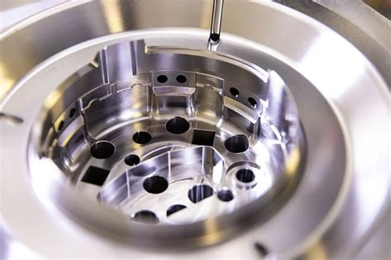
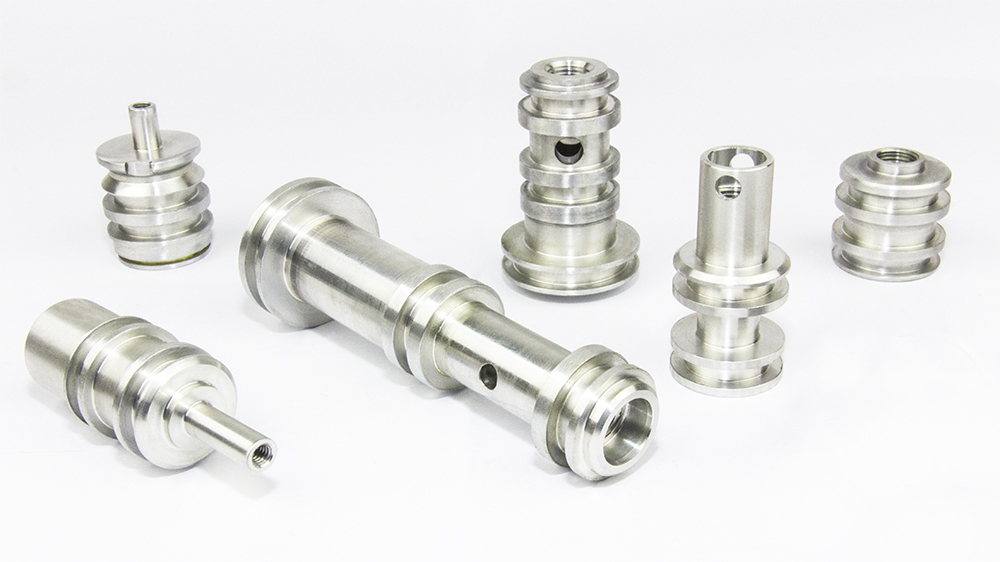
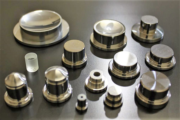
Precision Engineering for Complex Geometries
Vacuum metallizing of CNC-machined components presents unique challenges that require specialized engineering solutions.
Fixture Design for Uniform Deposition
The line-of-sight nature of many vacuum deposition processes necessitates strategic component positioning:
-
Rotational Fixtures: Planetary rotation systems with multiple axes ensure all surfaces receive uniform coating exposure
-
Shadowing Mitigation: Strategic placement minimizes self-shadowing on complex geometries with deep recesses or undercuts
-
Thermal Management: Fixtures designed with appropriate thermal mass and conductivity prevent temperature gradients that affect deposition rates
Thickness Uniformity Optimization
Achieving consistent coating thickness across complex components requires:
-
Source-to-Substrate Distance Optimization: Balancing deposition rate against throwing power for specific geometries
-
Shielding Design: Custom masks that selectively block deposition from areas where coating is undesirable
-
Process Parameter Tuning: Adjusting pressure, power, and gas flows to modify deposition characteristics
Stress Management in Coated Components
The mismatch in coefficient of thermal expansion (CTE) between substrate and coating generates interfacial stresses:
-
CTE Matching: Selecting coating materials with CTE values close to the substrate material
-
Graded Interfaces: Gradually changing composition from substrate to coating minimizes stress concentration
-
Post-deposition Annealing: Controlled thermal cycles relieve intrinsic stresses without degrading coating properties
Substrate Preparation for Optimal Adhesion
The performance of vacuum-metallized coatings is fundamentally determined by substrate surface conditions before deposition.
Surface Cleaning Protocols
-
Solvent Degreasing: Removal of oils and organic contaminants using sequential solvent baths (typically acetone, isopropyl alcohol)
-
Alkaline Cleaning: Chemical removal of organic residues and activation of metal surfaces
-
Acid Etching: Controlled surface roughening and oxide removal for enhanced mechanical interlocking
-
Ultrasonic Agitation: Cavitation-assisted cleaning of complex geometries and blind features
Surface Activation Techniques
-
Plasma Cleaning: In-situ argon or oxygen plasma treatment immediately before deposition removes adsorbed water and activates surface sites
-
Ion Bombardment: Low-energy ion etching creates nucleation sites and removes weak boundary layers
-
Chemical Primers: Specialized adhesion promoters for challenging substrate materials (plastics, ceramics)
Surface Roughness Optimization
-
Optimal Ra Range: 0.2-0.8 µm provides sufficient surface area for mechanical interlocking while maintaining coating continuity
-
Isotropic Finishes: Vapor honing or chemical etching creates uniform surface topography without directional patterns
-
Defect Elimination: Removal of burrs, microcracks, and inclusions that create stress concentrations
Table 3: Substrate Preparation Requirements by Material
| Substrate Material | Pretreatment Sequence | Optimal Surface Roughness | Adhesion Promotion | Special Considerations |
|---|---|---|---|---|
| Aluminum (6061, 7075) | 1. Alkaline clean 2. Acid etch (HF/HNO₃) 3. Deoxidize 4. DI rinse |
Ra 0.4-0.8 µm | Chromium or titanium adhesion layer (10-20 nm) | Remove heavy oxide layer; prevent reoxidation before coating |
| Stainless Steel | 1. Solvent degrease 2. Electroclean (alkaline) 3. Acid activate 4. Passivate |
Ra 0.2-0.6 µm | Chromium or nickel adhesion layer | Remove passivation layer without excessive roughening |
| Titanium | 1. Alkaline clean 2. Acid etch (HF/HNO₃) 3. DI rinse 4. Plasma clean |
Ra 0.3-0.7 µm | None typically required | Handle HF with extreme safety precautions |
| Engineering Plastics | 1. Solvent clean 2. Plasma treatment (O₂ or Ar) 3. Adhesion promoter |
Ra 0.5-1.0 µm | Silane or proprietary adhesion promoters | Control temperature during deposition to prevent distortion |
| Glass/Ceramics | 1. Piranha clean (H₂SO₄:H₂O₂) 2. DI rinse 3. Plasma clean |
Ra 0.1-0.4 µm | None typically required | Ensure complete removal of organic residues |
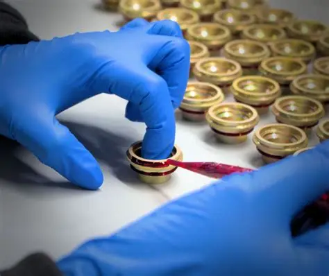
Quality Assurance and Performance Validation
Rigorous testing protocols ensure vacuum-metallized coatings meet specified performance requirements.
Adhesion Testing
-
Tape Test (ASTM D3359): Cross-hatch pattern with adhesive tape application and removal provides qualitative adhesion assessment
-
Scratch Testing: Progressive loading with diamond stylus determines critical load (Lc) for coating failure
-
Pull-Off Testing: Quantitative measurement of adhesion strength using bonded studs and tensile loading
Thickness Measurement
-
X-ray Fluorescence (XRF): Non-destructive measurement of coating thickness and composition
-
Ball Cratering (Calotester): Creates spherical crater through coating with thickness calculated from geometry
-
Cross-section SEM: Direct imaging of coating thickness and interface quality (destructive)
Functional Performance Testing
-
Electrical Conductivity: Four-point probe measurement of sheet resistance (Ω/□)
-
Optical Properties: Spectrophotometry for reflectivity, transmissivity, and color measurement
-
Corrosion Resistance: Salt spray testing (ASTM B117), electrochemical impedance spectroscopy
-
Barrier Properties: Water vapor transmission rate (WVTR) and oxygen transmission rate (OTR) measurements
Table 4: Vacuum Metallizing Quality Standards and Testing
| Quality Parameter | Test Method | Equipment/Standard | Typical Specification | Frequency |
|---|---|---|---|---|
| Coating Thickness | X-ray Fluorescence | Fischer XDV-SDD | ±10% of nominal thickness | First article & batch sampling |
| Adhesion Strength | Tape Test | ASTM D3359 | Class 4B or 5B | First article & each batch |
| Surface Resistivity | Four-point probe | Jandel RM3000 | <0.1 Ω/□ for conductive coatings | First article & batch sampling |
| Optical Reflectivity | Spectrophotometer | PerkinElmer Lambda 950 | >85% (visible) for reflective coatings | First article & quarterly |
| Corrosion Resistance | Salt Spray | ASTM B117 | 24-96 hours to first corrosion | First article & quarterly |
| Coating Composition | EDS/SEM | Thermo Scientific Apreo | Within 5% of target | First article & material change |
| Surface Roughness | Profilometry | Taylor Hobson PGI | Ra < 0.5 µm increase from substrate | First article & setup |
| Color Consistency | Spectrophotometer | X-Rite Ci64 | ΔE < 1.0 from master standard | Each production run |
Application-Specific Case Studies
Case Study 1: Aerospace Satellite Component Thermal Control Coating
Challenge: A satellite manufacturer needed precise thermal control surfaces with specific solar absorptance (αs) to emittance (ε) ratios (αs/ε = 0.20-0.80 depending on component location) to manage temperature extremes in orbit (±150°C).
Solution: We developed graded multilayer vacuum metallizing:
-
Adhesion Layer: 30 nm chromium deposited via DC magnetron sputtering
-
Functional Layers: Precisely controlled aluminum and SiO₂ layers with thicknesses tuned to achieve target αs/ε ratios
-
Protective Overcoat: 50 nm SiO₂ via reactive sputtering for atomic oxygen protection in low-earth orbit
Results: Components achieved αs/ε ratios within ±0.02 of specifications with excellent uniformity across complex geometries. Thermal cycling tests (-150°C to +120°C, 1000 cycles) showed no degradation in optical properties or adhesion.
Case Study 2: Medical Device EMI Shielding
Challenge: A portable medical monitoring device required 40 dB attenuation at 1-10 GHz while maintaining lightweight construction and biocompatibility for external use.
Solution: We implemented a conformal copper coating on complex plastic housing:
-
Surface Activation: Oxygen plasma treatment to create reactive sites on PEEK housing
-
Adhesion Layer: 20 nm chromium deposited via magnetron sputtering
-
Conductive Layer: 500 nm copper achieving sheet resistance of 0.03 Ω/□
-
Protective Layer: 100 nm gold flash for corrosion resistance and biocompatibility
Results: The vacuum-metallized housing provided 42-45 dB attenuation across the specified frequency range while adding only 8 grams to device weight. The coating passed ISO 10993 biocompatibility testing and showed no degradation after 500 sterilization cycles.
Case Study 3: Automotive Lighting Reflector Enhancement
Challenge: An automotive supplier needed to improve headlight reflector efficiency by 15% while reducing material costs and maintaining durability under harsh environmental conditions.
Solution: We optimized aluminum vacuum metallizing on injection-molded polymer reflectors:
-
Surface Preparation: Vapor honing to Ra 0.6 µm followed by plasma cleaning
-
Barrier Layer: 50 nm SiO₂ via reactive evaporation to prevent outgassing
-
Reflective Coating: 100 nm high-purity aluminum (99.999%) deposited via thermal evaporation with planetary rotation
-
Protective Overcoat: 5 µm UV-curable acrylic lacquer for abrasion and environmental protection
Results: Reflectors achieved 92% reflectivity (18% improvement over previous electroplated version) with 30% cost reduction. Environmental testing (2000 hours xenon arc, thermal cycling -40°C to 85°C) showed no degradation compared to electroplated controls.
The Future of Vacuum Metallizing Technology
Intelligent Deposition Systems
-
Machine Learning Process Control: AI algorithms optimizing deposition parameters in real-time based on in-situ monitoring
-
Digital Twin Integration: Virtual coating process simulation predicting outcomes before physical deposition
-
Adaptive Fixturing: Smart fixtures that adjust position based on real-time thickness monitoring
Advanced Material Systems
-
Metamaterial Coatings: Engineered structures with properties not found in natural materials
-
Self-healing Layers: Incorporation of microcapsules or reversible chemical bonds for damage repair
-
Responsive Coatings: Surfaces that change properties (wettability, conductivity) with environmental stimuli
Sustainable Vacuum Metallizing
-
Energy Efficiency: High-efficiency power supplies and improved vacuum system design reducing power consumption by 30-40%
-
Material Utilization Optimization: Advanced target designs and process controls increasing material utilization from 20-30% to 60-80%
-
Green Chemistry Alternatives: Development of non-toxic alternatives to currently used specialty materials
Conclusion: Surface Engineering as a Value Multiplier
Vacuum metallizing represents a critical surface engineering technology that extends component capabilities far beyond their substrate limitations. The ability to apply pure, adherent metallic coatings with precise thickness control enables solutions to complex engineering challenges in electronics, optics, aerospace, medical devices, and consumer products. Unlike conventional plating processes, vacuum metallizing operates without liquid chemicals, eliminating waste streams and environmental concerns while producing superior coatings.
The successful implementation of vacuum metallizing requires integrated expertise in vacuum physics, materials science, surface engineering, and precision manufacturing. At JLYPT, we’ve built our vacuum metallizing capabilities on this comprehensive foundation, viewing surface enhancement not as an ancillary process but as an essential component of complete manufacturing solutions.
Ready to enhance your components through advanced surface engineering? Contact our materials engineering team to discuss how our vacuum metallizing capabilities can address your most challenging performance requirements. From initial coating design through application and validation, we provide complete surface engineering solutions that improve performance, reduce costs, and enable new applications. Begin your surface enhancement project at JLYPT PVD Coating Services.