PVD Thin Film Technology: Revolutionizing Surface Finishing with Nano-Scale Precision
1. What Is PVD Thin Film Technology?
| Metric | PVD Thin Film | Traditional PVD | Electroplated Ni |
|---|---|---|---|
| Thickness Range | 5 nm–5 µm | 1–3 µm | 5–50 µm |
| Resolution | ±5 nm | ±50 nm | ±10 µm |
| Hardness (HV) | 2 500–3 500 | 2 000–3 000 | 700 |
| Max Service Temp | 1 000 °C | 400 °C | 300 °C |
| REACH Status | Compliant | Compliant | Restricted |
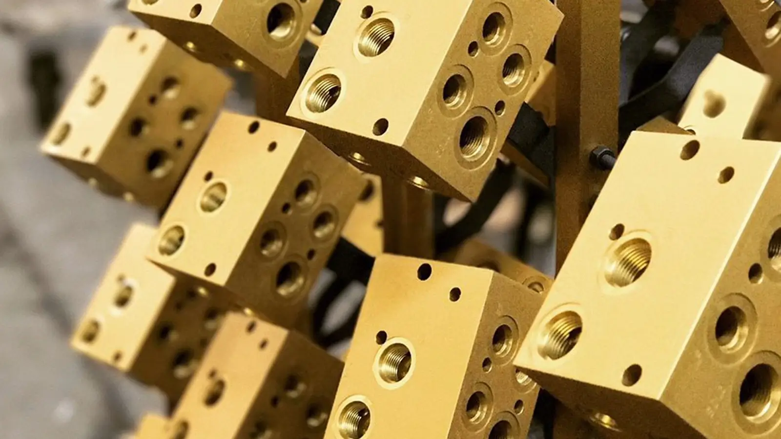
2. Core Processes – From Atoms to Angstroms
| Step | Vacuum Level | Temp (°C) | Key Action | KPI |
|---|---|---|---|---|
| 1 Plasma Clean | 10⁻³ mbar | 25 | Ar⁺ removes oxide & oil | Contact angle ≤ 8° |
| 2 Bond Layer | 10⁻³ mbar | 200 | 50 nm Cr or TiN for adhesion | Calot ±2 nm |
| 3 Nano-Deposition | 10⁻⁴ mbar | 150–500 | HiPIMS / Filtered Arc | ±5 nm uniformity |
| 4 Functional Stack | 10⁻⁴ mbar | 150–500 | Gradient TiAlCrN / ta-C DLC | 0.04 friction vs. steel |
| 5 Post-Polish | Air | 25 | Ion-beam Ra ≤ 0.01 µm | Optional |
| 6 QA & Pack | Air | 25 | CT + nano-indent + salt-spray | CpK ≥ 1.67 |
3. 2024 Performance Benchmark (Thin-Film PVD vs Legacy)
| Finish | Thickness (µm) | Hardness (HV) | Salt-Spray (h) | Max Temp (°C) | Cost / m² (USD) |
|---|---|---|---|---|---|
| Electroplated Ni | 25 | 700 | 48 | 300 | 2.5 |
| Spray Paint | 50 | 200 | 48 | 150 | 0.8 |
| Traditional DLC | 2 | 2 000 | 500 | 400 | 4.0 |
| HiPIMS TiAlCrN (thin-film PVD) | 2 | 2 900 | 1 200 | 1 000 | 3.2 |
| Filtered Arc ta-C (thin-film PVD) | 0.5 | 3 000 | 1 000 | 400 | 2.8 |
4. Three 2024 Case Studies
Case 1 – EV Motor Lamination Die
-
Challenge: 0.35 mm electrical steel sticking at 400 °C
-
Thin-Film Stack: 1.8 µm CrAlON + 50 nm a-C:H
-
Outcome: Tool life 4× longer, scrap −40 %
Case 2 – Medical Staple
-
Challenge: 316L needs low-friction piercing
-
Thin-Film Stack: 300 nm ta-C + 30 nm Cr adhesion
-
Outcome: Penetration force −25 %, CE mark granted
Case 3 – Smartphone EMI Shield
-
Challenge: 6 GHz EMI leakage in SiC inverter
-
Thin-Film Stack: 150 nm Ag/Ni/Cr multilayer
-
Outcome: Shielding 85 dB @ 6 GHz, CISPR 25 passed
5. Step-by-Step Thin-Film Workflow (7-Day Timeline)
| Milestone | Lead Time |
|---|---|
| DFM + Quote | 24 h |
| Prototype (1–10 pcs) | 48 h |
| Validation (CT, salt-spray) | 5 days |
| Mass Production | 7–10 days |
| Door-to-Door Delivery | 12 days total |
6. Global Standards & Sustainability
-
ISO 9001:2015 / IATF 16949 / ISO 13485
-
REACH, RoHS, FDA 21 CFR §175.300
-
Energy: 0.45 kWh per m²
-
Waste: Zero liquid effluent
7. FAQs – How Does Thin-Film PVD Work on …?
| Substrate | Answer |
|---|---|
| Steel | Standard HiPIMS TiAlCrN or CrN stack |
| Titanium | ta-C DLC for biocompatibility |
| Aluminum | CrAlON for 600 °C oxidation resistance |
| Plastics | Plasma-polymer adhesion + Ag/Ni EMI layer |
8. How to Start Your Thin-Film Project Tomorrow
-
Email [email protected] with STEP/IGES.
-
State substrate, load, temperature, thickness budget.
-
Receive DFM + thin-film stack + quote within 48 h.
-
Approve → 3-day prototype → volume ramp.
Explore complementary services: Professional Anodizing Near Me
Ready to turn atoms into performance?
Contact JLY Precision Tech—the China pvd thin film technology partner that ships tomorrow.
Contact JLY Precision Tech—the China pvd thin film technology partner that ships tomorrow.