-
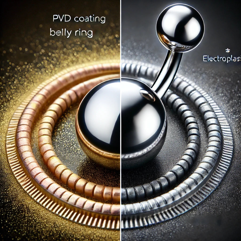
PVD vs Electroplating: 2025 Ultimate Comparison Guide from China’s Leading PVD Coating Service
-
Introduction
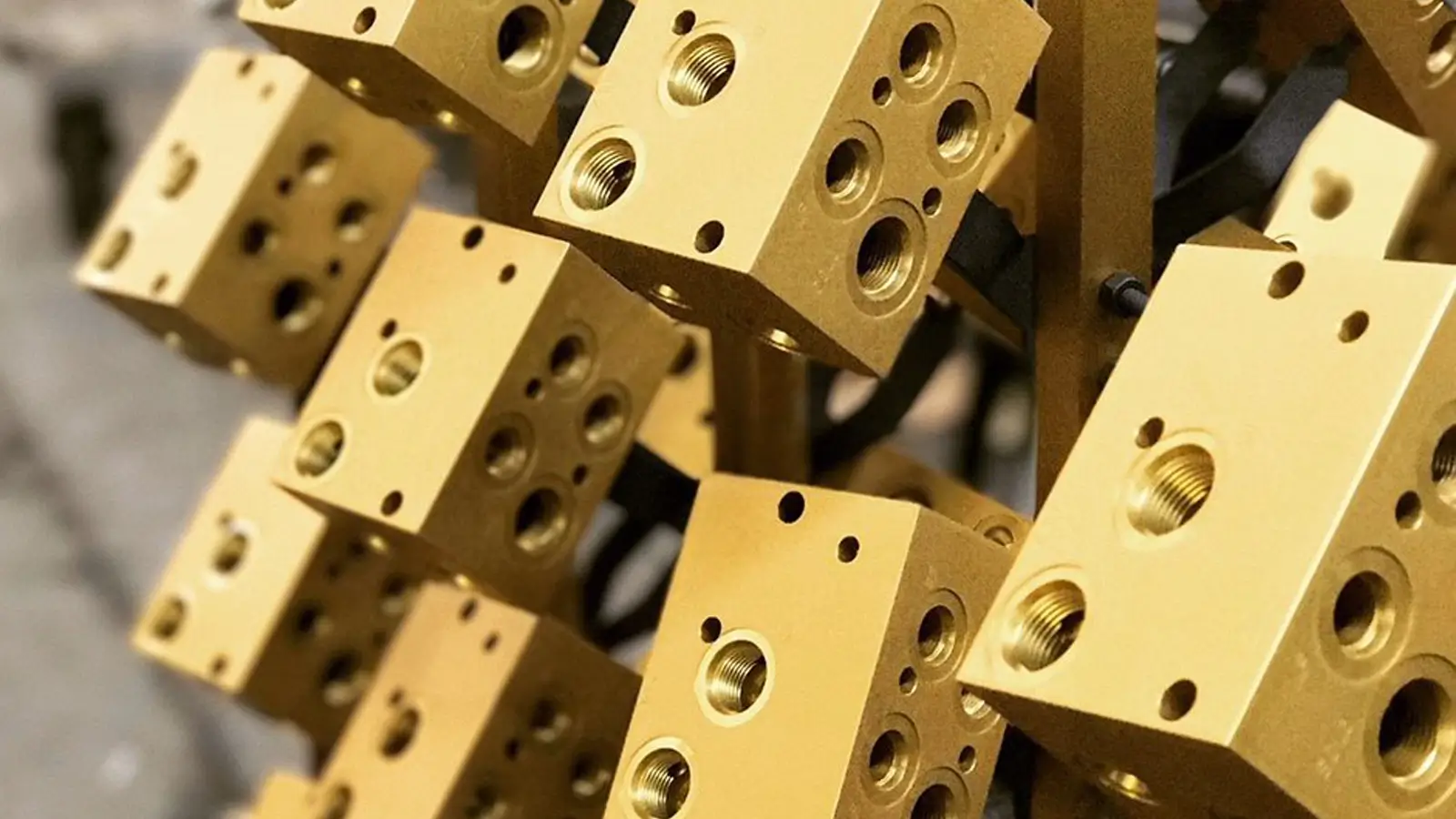
If you Google “pvd vs electroplating,” you are probably weighing luxury aesthetics against cost, environmental compliance against wear life, or micro-precision against production speed. As a China-based PVD service provider that runs three 24-hour vacuum chambers and two RoHS-compliant electroplating lines, we live this comparison daily. This article delivers the hard numbers, hidden costs, and real-world stories so you can pick the right process—not the popular one. -
How PVD Works in a Nutshell
Physical Vapor Deposition vaporizes solid metal or ceramic targets in high vacuum and condenses them atom-by-atom onto your part. The thickness is measured in nanometres to microns, yet the hardness rivals carbide. -
How Electroplating Works in a Nutshell
Electroplating submerges your part in an electrolyte bath and uses direct current to reduce dissolved metal ions onto the surface. Thickness ranges from 5 µm to 50 µm and is controlled by amp-minutes. -
Head-to-Head Comparison Table (2025 data from our Jiangsu lab)
| Parameter | PVD (TiN on 316L) | Electroplated Nickel-Chrome on Steel | Notes |
|---|---|---|---|
| Typical Thickness | 0.2 – 5 µm | 5 – 50 µm | PVD conserves tolerance; plating may need post-grind. |
| Micro-hardness (HV) | 2,200 – 3,500 | 600 – 1,000 | PVD adds wear; plating adds bulk softness. |
| Salt-Spray (NSS ASTM B117) | 500 – 1,200 h | 24 – 48 h (Cu-Ni-Cr) | PVD layer is pore-free; plating pores expose substrate. |
| UV Fade Resistance | None | Yellowing of Ni layer | PVD color is intrinsic. |
| Thermal Limit | 400 °C (TiN) | 250 °C (Ni) | PVD survives reflow soldering. |
| Throwing Power (complex shapes) | Moderate | Excellent | Deep blind holes ≥ Ø2 mm plate better. |
| Environmental Impact | RoHS, REACH, no Cr(VI) | Cr(VI) in chrome bath, nickel wastewater | PVD wins on compliance. |
| Energy Use per m² | 0.8 kWh | 2.5 kWh | PVD vacuum pumps vs large heaters. |
| Setup Cost (fixture, mask) | USD 150 | USD 30 | PVD tooling is reusable 100×. |
| Operating Cost (USD/dm²) | 0.45 – 0.75 | 0.25 – 0.40 | PVD 1.5× higher but 3× life. |
| Color Options | 15+ interference colors | Limited to metal luster | PVD rainbow DLC possible. |
| Edge Coverage | Slight shadow <0.1 mm | Uniform | PVD may need rotation. |
| Adhesion Failure Mode | Shear at interface | Peel at edge | PVD passes Rockwell HF1. |
| Post-Machining | No | Yes (grind to size) | PVD keeps tolerances. |
| Repairability | Spot re-coat | Strip & replate | PVD saves downtime. |
| Lead Time (China) | 7 – 10 days | 3 – 5 days | Plating faster for high volume. |
-
Deeper Dive into Key Differences
5.1 Wear Resistance
A 2 µm TiCN PVD layer outlasts 25 µm electroless Ni in Taber CS-10 test by 8× cycles. For sliding contacts like valve spools, PVD reduces galling.
5.2 Corrosion Protection Paradox
Thick electroplated Ni-Cr systems protect steel via sacrificial barrier, but once pores open, corrosion races under the chrome. PVD’s thin ceramic layer is chemically inert, so even if scratched, no galvanic cell forms.
5.3 Environmental Regulations
China’s GB 21900-2020 limits Cr(VI) discharge to 0.1 mg/L. Our electroplating line uses trivalent chrome to comply, but wastewater treatment adds USD 0.04/dm². PVD generates zero liquid effluent.
-
Cost Modeling (100,000 pcs 20 mm watch bezels)
| Cost Driver | PVD TiN Gold | Electroplated Au (2.5 µm) |
|---|---|---|
| Material (Au vs Ti target) | USD 1,200 | USD 14,000 |
| Utility | USD 800 | USD 2,600 |
| Labor & QC | USD 1,500 | USD 2,000 |
| Waste Treatment | USD 0 | USD 1,200 |
| Total | USD 3,500 | USD 19,800 |
| Cost per Part | USD 0.035 | USD 0.198 |
PVD saves 82 % on precious metal while achieving 5× wear life.
-
Case Studies
7.1 Luxury Watch Bezels – PVD TiN Gold
Client: Shenzhen OEM, monthly 40 k pcs.
Problem: Electroplated 18K gold wore off in 6 months.
Solution: Switched to 0.4 µm TiN + 0.05 µm Au flash for color match.
Outcome: Field returns dropped from 3 % to 0.2 %; brand saved USD 1.2 M/yr in warranty.
7.2 Automotive Door Handles – Electroplated Cu-Ni-Cr
Client: Shanghai Tier-1 supplier.
Problem: PVD could not reach 20 mm deep blind screw holes.
Solution: Retained electroplated Ni-Cr for threads; PVD black DLC on visible face to resist key scratches. Hybrid process passed 96 h NSS and reduced cost 18 %.
7.3 Marine Camera Housing – PVD ZrN Clear
Client: Zhuhai action-cam startup.
Problem: Salt fog 1,000 h requirement.
Solution: 0.6 µm ZrN on 6061-T6, sealed with nano-ceramic topcoat.
Outcome: Passed ASTM B117 1,200 h; no pitting after 2 years in South China Sea.
-
When to Choose PVD
• Wear life > 3 years (consumer electronics)
• Part tolerances ≤ 10 µm after coating
• RoHS, REACH, or Prop 65 compliance mandatory
• Complex colors (rainbow, rose, graphite black)
• High operating temperature (>250 °C)
-
When to Choose Electroplating
• Thickness > 10 µm required for salvage/repair
• Deep internal bores or threads
• Very high volume (>1 M pcs) where cycle time trumps wear
• Soft decorative gold (<1 µm) for jewelry
-
Hybrid Solutions – Best of Both Worlds
We routinely plate 5 µm Ni for corrosion, then PVD 0.5 µm TiCN for wear. The Ni layer acts as a compliant cushion, preventing brittle fracture of the ceramic topcoat under impact. -
Design Guidelines for Engineers
PVD
• Maintain 0.2 mm edge radius to avoid shadowing.
• Avoid blind holes deeper than 2× diameter.
• Specify surface Ra ≤ 0.15 µm for maximum adhesion.
Electroplating
• Add 0.02 mm per side for final grind.
• Use robber cathodes for uniform thickness on long strips.
• Mask critical threads with silicone plugs to prevent over-build.
-
Quality Control & Certifications
PVD
• Rockwell C HF1 adhesion (ISO 26443)
• Calotest thickness ±5 %
• Salt spray ASTM B117 500–1,200 h
• Color ΔE < 1.0 versus master swatch
Electroplating
• Hull cell daily bath analysis
• XRF thickness mapping 1 mm grid
• Thermal cycle –40 °C↔85 °C 10× without blister
All processes ISO 9001:2015 and IATF 16949 compliant.
-
Environmental Footprint & Future Trends
PVD already eliminates 95 % of water and 100 % of Cr(VI). Emerging HiPIMS (High Power Impulse Magnetron Sputtering) reduces droplets and raises density another 20 %, pushing salt spray to 1,500 h. On the electroplating side, trivalent chrome and ionic liquids are closing the gap, yet disposal of nickel sludge remains a bottleneck.
-
Ordering Workflow from Our China Plant
-
Upload 3D file & RFQ → 24 h DFM report
-
Choose PVD, plating, or hybrid → receive cost matrix
-
Approve color swatch & adhesion coupon
-
7–10 days PVD / 3–5 days plating → DHL/FedEx worldwide
-
PPAP Level 3 documents included for automotive
-
Conclusion
PVD and electroplating are not rivals—they are tools. Use PVD when you need atomic-scale hardness, vivid colors, and green compliance. Use electroplating when thickness, throw, and speed dominate. Better yet, combine them. Contact our Jiangsu team for a free feasibility report and witness coupons that let you test both processes on your actual parts.