Precision Engineering for the Digital Age: Semiconductor Tooling and Precision Component Supplier Expertise
The semiconductor manufacturing industry represents the pinnacle of human technological achievement, where atomic-scale precision meets industrial-scale production. Within this ecosystem, the performance and reliability of processing equipment directly determine yield, throughput, and ultimately, the economic viability of entire fabrication facilities. At JLYPT CNC Machining, we have established ourselves as a premier semiconductor tooling and precision component supplier by mastering the unique intersection of extreme precision, material science, and contamination control required for semiconductor manufacturing applications.
This comprehensive technical analysis explores the sophisticated manufacturing methodologies, specialized materials, and rigorous quality protocols that define excellence as a semiconductor tooling and precision component supplier. We will examine how advanced CNC technologies, when combined with specialized post-processing and metrology capabilities, enable the production of components that meet the extraordinary demands of wafer processing equipment operating at the frontiers of Moore’s Law.
The Extraordinary Demands of Semiconductor Manufacturing Environments
Semiconductor fabrication equipment presents challenges that dwarf those of conventional precision manufacturing. Components must perform flawlessly in environments that push the boundaries of physics and materials science:
Ultra-High Vacuum and Process Chamber Compatibility
Semiconductor processes occur in environments where even minute contamination can destroy product yield. Components must maintain integrity in:
-
High-Vacuum Conditions: Operating in environments from 10⁻⁵ to 10⁻¹¹ Torr demands exceptional outgassing properties and precise dimensional stability
-
Plasma Environments: Withstanding ion bombardment and radical species in etch, deposition, and cleaning chambers without particle generation
-
Extreme Thermal Cycling: Maintaining dimensional stability across temperature ranges from cryogenic to over 1000°C during thermal processing
-
Chemical Compatibility: Resisting corrosion from aggressive process chemicals including HF, HCl, O₂, and various halogen gases
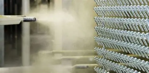
Particulate Control and Cleanroom Manufacturing
The transition to smaller process nodes has made particulate contamination an increasingly critical concern. As a dedicated semiconductor tooling and precision component supplier, we implement comprehensive contamination control protocols:
-
ISO Class 4-7 Cleanroom Manufacturing: All critical components are machined and assembled in controlled environments with particulate monitoring
-
Specialized Material Handling: Components are protected throughout manufacturing using static-dissipative packaging and cleanroom-compatible handling procedures
-
Surface Finish Optimization: Achieving surface finishes better than Ra 0.2 μm to minimize particle adhesion and facilitate thorough cleaning
-
Electropolishing and Passivation: Specialized surface treatments to create non-reactive, smooth surfaces that resist particle accumulation
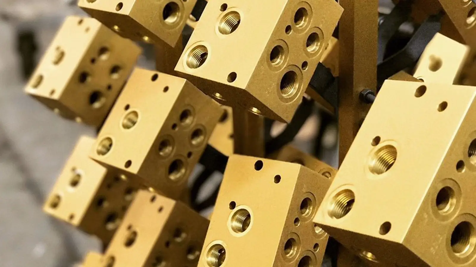
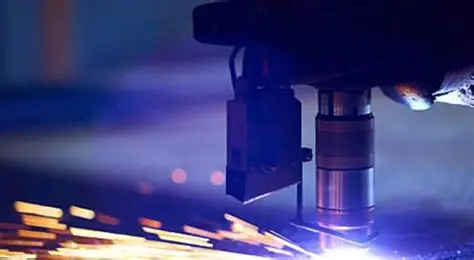
Advanced Manufacturing Technologies for Semiconductor Applications
The extreme requirements of semiconductor tooling demand specialized manufacturing approaches beyond conventional precision machining. Our technology portfolio is specifically tailored to meet these challenges:
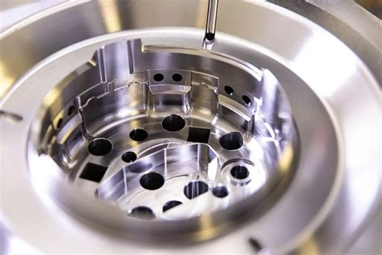
5-Axis Simultaneous Machining for Complex Geometries
For components with complex internal channels, contoured surfaces, and critical interface features, 5-axis simultaneous machining provides essential capabilities:
-
Single-Setup Machining: Complete processing of complex parts eliminates handling contamination and maintains exceptional feature relationships
-
Complex Internal Passage Machining: Production of cooling channels, gas distribution paths, and vacuum ports with uninterrupted toolpaths
-
Optimized Tool Engagement: Continuous 5-axis movement maintains ideal cutting conditions for superior surface finishes without hand polishing
-
True Positional Accuracy: Maintaining precise feature relationships across complex part geometries without cumulative error
Precision Micro-Machining for Miniature Features
As semiconductor features shrink below 5nm, tooling components require correspondingly smaller features with exceptional precision:
-
Micro-Tool Expertise: Machining with tools as small as 0.1mm diameter for intricate features and high-aspect-ratio geometries
-
High-Speed Spindles: Spindles capable of 60,000+ RPM maintain proper surface speeds with micro-tools for optimal surface integrity
-
Vibration Control: Specialized machine foundations and tooling systems eliminate vibrations that compromise micro-feature accuracy
-
Sub-Micron Precision: Achieving positional accuracy better than 1μm for critical alignment and interface features
Multi-Axis Mill-Turn Machining for Rotational Components
For components requiring both rotational symmetry and complex off-axis features, our multi-axis mill-turn centers provide complete solutions:
-
Complete Part Processing: Turning, milling, drilling, and threading operations in single setup minimizes handling and contamination risk
-
Complex Feature Integration: Machining of non-radial ports, mounting features, and alignment structures on cylindrical components
-
Concentricity Control: Maintaining exceptional rotational accuracy for components requiring high-speed balance or precise alignment
-
Efficient Production: Reduced handling between operations decreases particulate generation risk and improves throughput
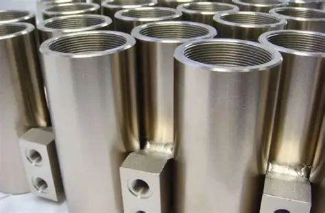
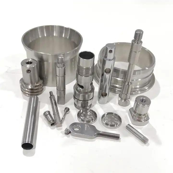
Critical Materials for Semiconductor Applications
Material selection represents a foundational consideration in semiconductor tooling design. Our expertise encompasses the specialized materials required for these demanding applications:
Aluminum Alloys for Structural Components
-
6061-T6 Aluminum: General-purpose structural components with good machinability and anodizing compatibility
-
7075-T6 Aluminum: High-strength applications where stiffness and strength-to-weight ratio are critical
-
5000 Series Aluminum: Superior corrosion resistance for components exposed to aggressive chemical environments
Stainless Steels for High-Strength Applications
-
304/304L Stainless Steel: Excellent general corrosion resistance with good formability and weldability
-
316/316L Stainless Steel: Enhanced corrosion resistance for components exposed to chloride environments
-
17-4PH Stainless Steel: Precipitation-hardening grade offering high strength and good corrosion resistance
-
440C Stainless Steel: High hardness and wear resistance for moving components and bearing surfaces
Exotic Alloys for Extreme Environments
-
Titanium Alloys: Exceptional strength-to-weight ratio and corrosion resistance for critical structural components
-
Inconel 718: Outstanding high-temperature strength and corrosion resistance for thermal processing components
-
Hastelloy C-22: Superior resistance to aggressive chemical environments including chlorine and fluorine plasmas
Critical Semiconductor Applications and Manufacturing Solutions
The table below details specific semiconductor manufacturing applications and the specialized manufacturing approaches required for each:
| Application Area | Critical Requirements | Material Selection | Manufacturing Approach |
|---|---|---|---|
| Wafer Handling Robots | Minimal particle generation, high stiffness-to-weight ratio, vacuum compatibility | 6061 Aluminum (hardcoat anodized), 316L Stainless Steel | 5-axis machining of complex arm structures, precision bearing fits, specialized surface treatments |
| Electrostatic Chucks | Flatness, thermal stability, dielectric properties, micro-feature accuracy | Aluminum Nitride, Aluminum (anodized), Ceramic composites | Ultra-precision machining, lapping to sub-micron flatness, specialized electrode patterning |
| Gas Distribution Systems | Complex internal passages, chemical compatibility, leak-free operation | 316L Stainless Steel, Hastelloy, Aluminum (anodized) | Deep-hole drilling, diffusion welding, electropolishing, helium leak testing |
| Process Chamber Components | Plasma resistance, thermal stability, minimal contamination | Aluminum (hardcoat anodized), 316L Stainless Steel, Silicon Carbide | 5-axis machining of complex shrouds, specialized surface treatments, vacuum baking |
| Optical Mounting Systems | Thermal stability, precise geometric control, vibration damping | Invar, Aluminum, Stainless Steel | Stress-relieved machining, thermal cycling, precision boring and threading |
| Vacuum Chamber Flanges | Flatness, surface finish, vacuum integrity, dimensional stability | 304/316 Stainless Steel, Aluminum | Precision facing, groove machining, specialized sealing surface finishes |
For comprehensive understanding of semiconductor equipment standards and material requirements, we regularly consult resources from SEMI International Standards to ensure compliance with industry specifications.
Comprehensive Case Studies: Semiconductor Manufacturing Solutions
Case Study 1: Silicon Electrostatic Chuck Manufacturing
-
Challenge: A semiconductor equipment manufacturer required precision electrostatic chucks for their advanced etch system. The components needed to maintain 2μm flatness across 300mm diameter, incorporate complex cooling channels, and provide reliable wafer clamping at elevated temperatures up to 200°C.
-
Manufacturing Solution: We manufactured the chuck bodies from vacuum-compatible aluminum with hardcoat anodized surfaces. The cooling channels were machined using 5-axis strategies with specialized tooling to maintain wall thickness consistency. Critical mounting surfaces were lapped to achieve the required flatness specification.
-
Technical Outcomes: The completed electrostatic chucks achieved 1.8μm flatness across the entire surface, with cooling channels demonstrating uniform flow distribution. The components passed helium leak testing at 1×10⁻¹⁰ mbar·L/s and showed no particle generation during extended testing. The improved thermal uniformity contributed to 3% better etch rate consistency across the wafer.
-
Internal Link: Discover our capabilities for complex semiconductor components through our Precision CNC Machining Services.
Case Study 2: Chemical Vapor Deposition Gas Distribution Plate
-
Challenge: A deposition tool manufacturer needed to upgrade their gas distribution system for improved film uniformity. The new design required thousands of precision micro-holes with diameters maintained within ±5μm, complex internal gas channels, and exceptional surface finish to prevent particle accumulation.
-
Manufacturing Solution: We employed precision micro-machining with specialized drill bits and optimized peck cycling to produce the required hole patterns. The internal gas manifold was created using diffusion-bonded layers with laser-etched channels. The entire assembly underwent electropolishing to achieve Ra 0.1μm surface finish.
-
Technical Outcomes: The gas distribution plate demonstrated hole diameter consistency of ±3μm with perfect circularity. The improved gas distribution resulted in 15% better film thickness uniformity across 300mm wafers. The component passed extended particle testing with zero added contamination over 1000-hour continuous operation.
-
External Resource: For detailed information on semiconductor gas system materials, we reference resources from ASM Materials Engineering.
Case Study 3: Wafer Handling Robot End Effector
-
Challenge: A robotics company specializing in wafer handling needed end effectors for 450mm wafer processing that could operate at high speeds without particle generation while maintaining exceptional dimensional stability across thermal cycles.
-
Manufacturing Solution: We designed and manufactured the end effectors from carbon fiber composite with titanium mounting interfaces. The complex contour was achieved through 5-axis machining of composite preforms followed by precision finishing. Critical wafer contact features were manufactured using ceramic components with specialized coatings.
-
Technical Outcomes: The end effectors achieved 60% weight reduction compared to aluminum designs while maintaining equivalent stiffness. The components demonstrated zero particle generation during extended testing and maintained positional accuracy within 10μm across the operational temperature range. The solution enabled 25% faster wafer transfer times while improving placement accuracy.
Quality Assurance and Metrology for Semiconductor Applications
The development of semiconductor tooling demands validation methodologies that ensure reliability in critical manufacturing environments:
-
CMM Verification: Comprehensive dimensional validation using coordinate measuring machines with sub-micron capability for critical features
-
Surface Metrology: White light interferometry and profilometry to validate surface finish and texture parameters
-
Cleanliness Validation: Particle counting and analysis to ensure components meet cleanliness specifications
-
Vacuum Testing: Helium leak detection and outgassing measurement to verify vacuum integrity
-
Material Verification: Composition analysis and mechanical testing to validate material properties
The Future of Semiconductor Tooling Manufacturing
The field of semiconductor tooling continues to evolve with emerging technologies and methodologies:
-
Additive Manufacturing Integration: Using metal additive manufacturing for conformal cooling channels and optimized structures combined with precision machining
-
Advanced Coating Technologies: Developing specialized coatings for improved plasma resistance and reduced particle generation
-
AI-Driven Process Optimization: Implementing machine learning for predictive maintenance and process optimization in tooling manufacturing
-
Quantum Manufacturing: Developing manufacturing approaches for quantum computing components with unprecedented precision requirements
-
Sustainable Manufacturing: Implementing environmentally conscious manufacturing processes without compromising performance
Conclusion: Precision as Standard in Semiconductor Tooling
The manufacturing of semiconductor tooling and precision components represents one of the most demanding applications of precision engineering. Success requires more than advanced machining capabilities—it demands deep understanding of materials science, contamination control, vacuum technology, and the specific requirements of semiconductor processing environments.
At JLYPT CNC Machining, our approach as a semiconductor tooling and precision component supplier combines technical expertise with practical semiconductor industry experience. We understand that nanometer-scale device features demand micron-scale tooling precision, and that component reliability directly impacts multi-million dollar fabrication operations. By integrating advanced manufacturing technologies with rigorous quality validation and contamination control, we deliver components that meet the extraordinary demands of the semiconductor industry.
Ready to enhance your semiconductor equipment with precision-engineered components? Contact JLYPT CNC Machining today to discuss how our expertise as a semiconductor tooling and precision component supplier can help you achieve your performance and reliability goals with components manufactured to the highest standards of precision and quality.