Thin Film Coating | PVD Surface Finishing China – JLY Precision Tech
1. What is Thin Film Coating in Surface Finishing?
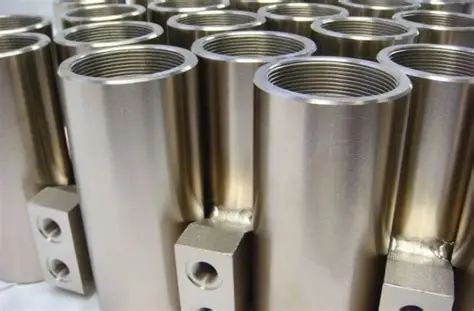
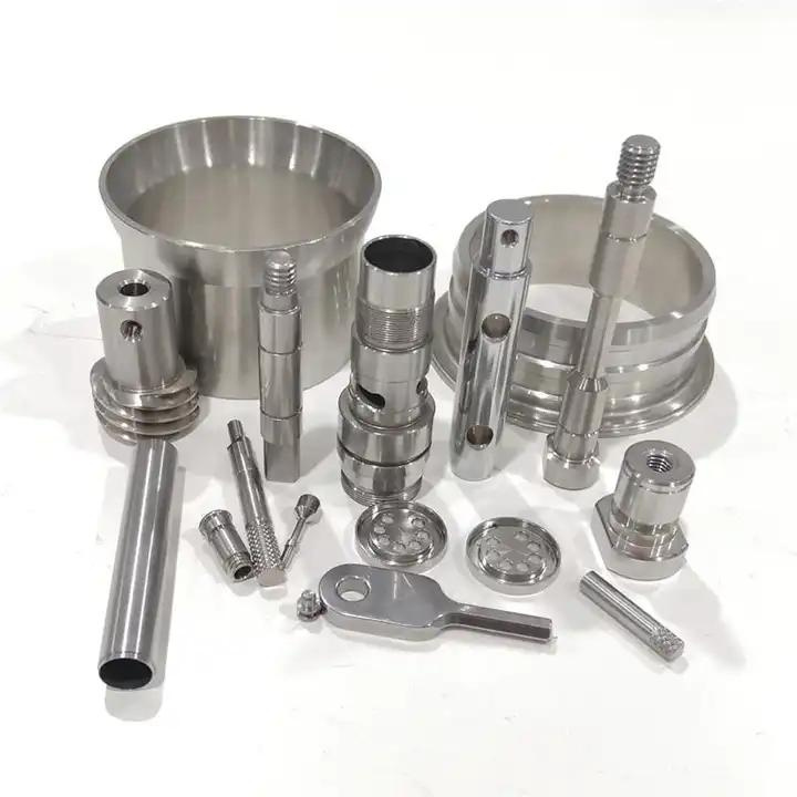
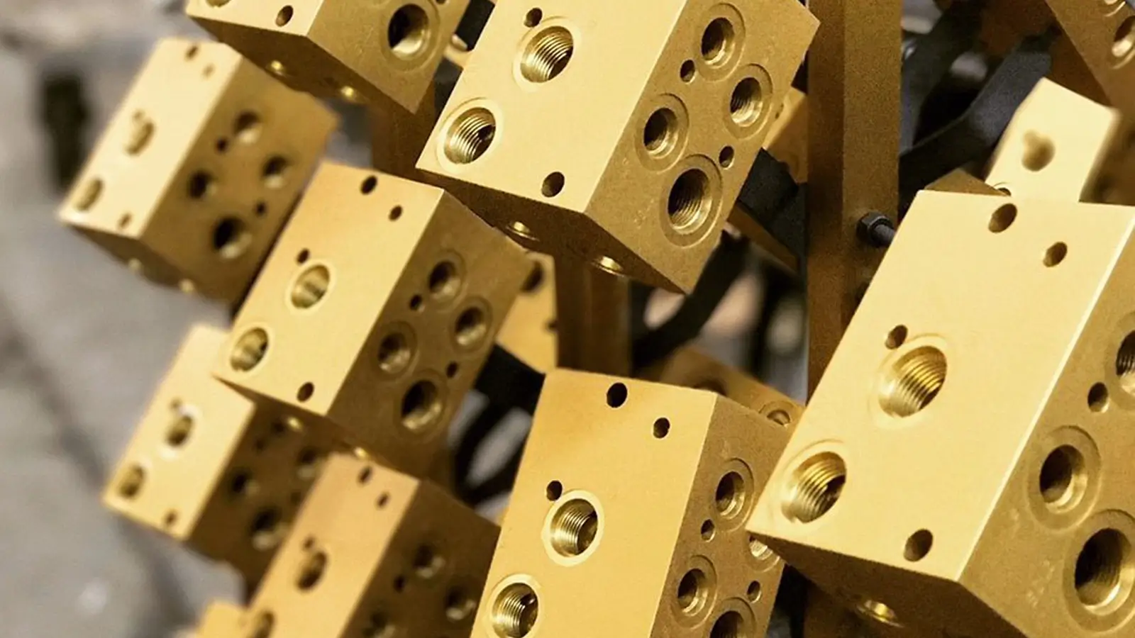
Thin film coating is a critical process in various industries, particularly in manufacturing and technology. This method involves depositing a very thin layer of material onto a substrate, enhancing the surface properties of the material. For example, in electronics, thin film coatings can be added to semiconductors to improve their performance and durability, affecting how devices operate in everyday use. Further, this technique is widely utilized in the automotive and aerospace industries to provide additional strength and resistance to the parts being coated. In this section, we will delve deeper into the specifics of thin film coating, exploring its applications and advantages.
| Definition | Why It Matters |
|---|---|
| Films < 5 µm deposited by PVD or ALD | Preserves micron-level tolerances |
| Multilayer stacks (metal + ceramic + DLC) | Tailored optical, thermal or tribological properties |
| Atomically bonded to substrate | No risk of peeling under thermal cycles |
Key Thin Film Coating Families We Offer
Understanding the various types of thin film coatings available is essential for selecting the right one for your application. Each type has unique properties tailored for specific uses. For example, optical coatings can enhance light transmission, while wear-resistant coatings can extend the life of components subjected to friction and abrasion. Additionally, multilayer coatings can be engineered to achieve unique optical or physical properties by layering different materials.
| Family | Typical Composition | Thickness Range | Primary Benefit |
|---|---|---|---|
| Oxides | Al₂O₃, TiO₂, SiO₂ | 0.1–2 µm | Electrical insulation & optical AR |
| Nitrides | TiN, CrN, TiAlN | 0.5–4 µm | Hardness 2 000–3 000 HV |
| Carbides | TiC, WC/C | 0.2–3 µm | Ultra-low friction 0.05–0.15 |
| Metals | Cr, Al, Ag | 0.05–1 µm | EMI shielding or reflectivity |
| DLC | ta-C, a-C:H | 0.5–4 µm | Bio-inert & wear-proof |
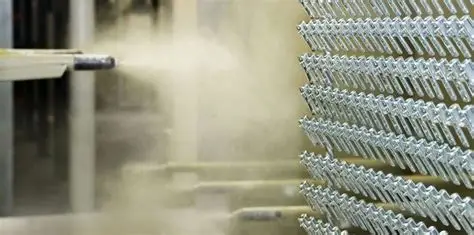
2. PVD Techniques for Thin Film Coating
Physical Vapor Deposition (PVD) techniques are critical for applying thin film coatings in modern manufacturing. These methods offer precise control over the coating process, allowing for the deposition of uniform layers on complex geometries. For instance, Magnetron Sputtering is particularly favored for its ability to create high-quality coatings at lower temperatures, which is essential for sensitive substrates. In contrast, Cathodic Arc techniques can deposit thicker films rapidly, making them suitable for applications requiring robust coatings.
| Method | Working Principle | Coating Uniformity | Best For |
|---|---|---|---|
| Magnetron Sputtering | Argon plasma bombards target | ±3 % across 600 mm | Optical multilayer |
| Cathodic Arc | Arc evaporates alloy cathode | ±5 % | High-rate TiAlN on tools |
| HiPIMS | High-power impulse sputtering | ±2 % | Dense CrN on dies |
| Filtered Arc | Plasma bends through magnetic filter | ±1 % | Ultra-smooth ta-C DLC |
3. Thin Film Coating Performance Matrix (2024 Data)
The performance of thin film coatings can be assessed through a matrix of characteristics, including hardness, friction properties, and resistance to environmental factors. This performance matrix allows manufacturers to choose the appropriate coating based on specific performance requirements. For example, a coating that excels in hardness may be ideal for cutting tools, while a coating with low friction properties might be better suited for moving parts in machinery.
| Stack on 316 SS | Thickness (µm) | Hardness (HV) | Salt Spray (h) | Friction vs. 100Cr6 | Max Temp (°C) |
|---|---|---|---|---|---|
| TiAlN / CrN | 2.5 | 2 800 | 1 000 | 0.25 | 850 |
| Al₂O₃ / TiO₂ AR | 0.25 | 1 200 | 500 | — | 600 |
| ta-C DLC | 1.0 | 3 000 | 1 200 | 0.05 | 400 |
| Ag / TiW | 0.1 | 300 | 48 | — | 200 |
4. Three Case Studies (2024)
In addition to the case studies mentioned, there are numerous real-world applications of thin film coatings that illustrate their importance. For instance, in the aerospace industry, thin film coatings are applied to turbine blades to improve their efficiency and extend their service life. The challenge of thermal fatigue is mitigated by using advanced coatings that withstand extreme temperatures and corrosive environments.
Case Study 1 – Smartphone Camera Lens AR Thin Film
Challenge: Reduce ghosting in 108 MP sensor.
Solution: 6-layer SiO₂/TiO₂ sputtered AR coating, 0.2 µm total, < 0.2 % reflection @ 550 nm.
Result: 12 % boost in low-light photo quality; 2.5 M lenses shipped.
Case Study 2 – Electric Motor Lamination Dies
Challenge: Sticking of 0.35 mm electrical steel causing burrs.
Solution: 1.5 µm CrN + 50 nm a-C:H top on D2 tool steel.
Result: Tool life 3× longer; downtime cut 60 %.
Case Study 3 – Disposable Surgical Staples
Challenge: 316L staples must pierce tissue without galling.
Solution: 300 nm ta-C DLC with Cr inter-layer.
Result: Force to fire reduced 30 %; CE mark granted.
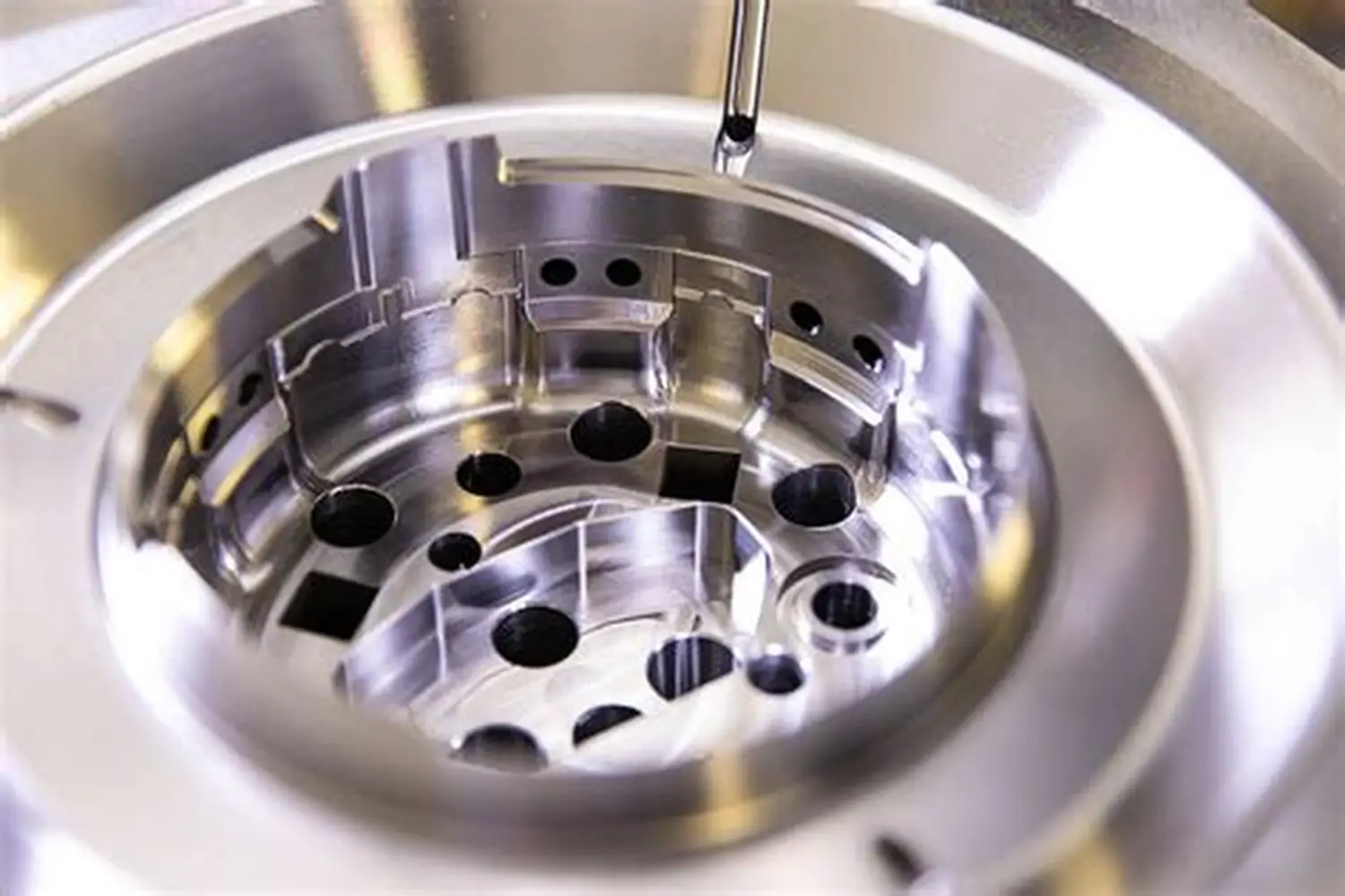
5. Step-by-Step Process Flow
| Step | Action | QC Check | Lead Time |
|---|---|---|---|
| RFQ Review | DFM, load modelling | 24 h | — |
| Substrate Clean | Plasma + ultrasonic | Contact angle ≤ 10° | 2 h |
| PVD Coating | Real-time thickness | ±5 nm | 3–6 h |
| Post-Polish | CMP optional | Ra ≤ 0.01 µm | 1 h |
| Final QA | Calot, nano-indentation | CpK ≥ 1.67 | 12 h |
6. Industry Outlook 2024-2027
The outlook for the thin film coating industry is promising, with advancements in technology driving adoption across various sectors. As industries look to enhance product performance and reduce costs, the demand for innovative coating solutions continues to grow. For example, the integration of AI and machine learning in the coating process is expected to optimize layer deposition, improve quality control, and reduce waste.
| Sector | 2024 Adoption | 2027 Forecast | Driving Need |
|---|---|---|---|
| Consumer Electronics | 15 % | 38 % | Thinner AR & EMI layers |
| Medical Implants | 22 % | 45 % | Bio-inert coatings |
| EV Motors | 8 % | 30 % | Lamination die release |
7. Frequently Asked Questions
Frequently asked questions about thin film coatings reveal common concerns among potential users. One of the most common questions is about the durability of thin film coatings, particularly in harsh environments. Users often want to know how these coatings perform under extreme conditions, such as high temperatures or corrosive atmospheres. The answers to these questions can significantly impact the decision-making process for manufacturers considering thin film technology for their products.
A: Yes. Plasma etch strips < 2 µm DLC without dimensional change.
A: Our SiO₂/TiO₂ stacks pass 134 °C steam 100 cycles with < 1 % reflectance shift.
A: No MOQ; prototypes start at 1 piece.
8. How to Order Today
-
Email [email protected] with STEP/IGES files.
-
Specify substrate, operating environment, thickness budget.
-
Receive DFM + coating stack + price within 48 h.
-
Approve → 3-day prototype → volume ramp.