
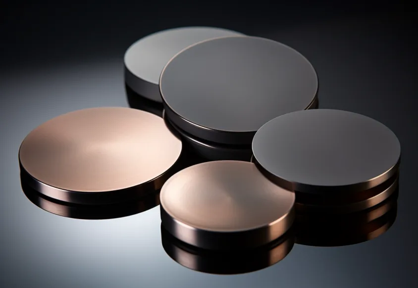
PVD Thin Film Technology: Revolutionizing Surface Finishing with Nano-Scale Precision
1. What Is PVD Thin Film Technology?
| Metric | PVD Thin Film | Traditional PVD | Electroplated Ni |
|---|---|---|---|
| Thickness Range | 5 nm–5 µm | 1–3 µm | 5–50 µm |
| Resolution | ±5 nm | ±50 nm | ±10 µm |
| Hardness (HV) | 2 500–3 500 | 2 000–3 000 | 700 |
| Max Service Temp | 1 000 °C | 400 °C | 300 °C |
| REACH Status | Compliant | Compliant | Restricted |
2. Core Processes – From Atoms to Angstroms
| Step | Vacuum Level | Temp (°C) | Key Action | KPI |
|---|---|---|---|---|
| 1 Plasma Clean | 10⁻³ mbar | 25 | Ar⁺ removes oxide & oil | Contact angle ≤ 8° |
| 2 Bond Layer | 10⁻³ mbar | 200 | 50 nm Cr or TiN for adhesion | Calot ±2 nm |
| 3 Nano-Deposition | 10⁻⁴ mbar | 150–500 | HiPIMS / Filtered Arc | ±5 nm uniformity |
| 4 Functional Stack | 10⁻⁴ mbar | 150–500 | Gradient TiAlCrN / ta-C DLC | 0.04 friction vs. steel |
| 5 Post-Polish | Air | 25 | Ion-beam Ra ≤ 0.01 µm | Optional |
| 6 QA & Pack | Air | 25 | CT + nano-indent + salt-spray | CpK ≥ 1.67 |
3. 2024 Performance Benchmark (Thin-Film PVD vs Legacy)
| Finish | Thickness (µm) | Hardness (HV) | Salt-Spray (h) | Max Temp (°C) | Cost / m² (USD) |
|---|---|---|---|---|---|
| Electroplated Ni | 25 | 700 | 48 | 300 | 2.5 |
| Spray Paint | 50 | 200 | 48 | 150 | 0.8 |
| Traditional DLC | 2 | 2 000 | 500 | 400 | 4.0 |
| HiPIMS TiAlCrN (thin-film PVD) | 2 | 2 900 | 1 200 | 1 000 | 3.2 |
| Filtered Arc ta-C (thin-film PVD) | 0.5 | 3 000 | 1 000 | 400 | 2.8 |
4. Three 2024 Case Studies
Case 1 – EV Motor Lamination Die
-
Challenge: 0.35 mm electrical steel sticking at 400 °C
-
Thin-Film Stack: 1.8 µm CrAlON + 50 nm a-C:H
-
Outcome: Tool life 4× longer, scrap −40 %
Case 2 – Medical Staple
-
Challenge: 316L needs low-friction piercing
-
Thin-Film Stack: 300 nm ta-C + 30 nm Cr adhesion
-
Outcome: Penetration force −25 %, CE mark granted
Case 3 – Smartphone EMI Shield
-
Challenge: 6 GHz EMI leakage in SiC inverter
-
Thin-Film Stack: 150 nm Ag/Ni/Cr multilayer
-
Outcome: Shielding 85 dB @ 6 GHz, CISPR 25 passed
5. Step-by-Step Thin-Film Workflow (7-Day Timeline)
| Milestone | Lead Time |
|---|---|
| DFM + Quote | 24 h |
| Prototype (1–10 pcs) | 48 h |
| Validation (CT, salt-spray) | 5 days |
| Mass Production | 7–10 days |
| Door-to-Door Delivery | 12 days total |
6. Global Standards & Sustainability
-
ISO 9001:2015 / IATF 16949 / ISO 13485
-
REACH, RoHS, FDA 21 CFR §175.300
-
Energy: 0.45 kWh per m²
-
Waste: Zero liquid effluent
7. FAQs – How Does Thin-Film PVD Work on …?
Running in vacuum explains most of the cost. The process step by step is set out in how PVD coating works.
| Substrate | Answer |
|---|---|
| Steel | Standard HiPIMS TiAlCrN or CrN stack |
| Titanium | ta-C DLC for biocompatibility |
| Aluminum | CrAlON for 600 °C oxidation resistance |
| Plastics | Plasma-polymer adhesion + Ag/Ni EMI layer |
8. How to Start Your Thin-Film Project Tomorrow
-
Email [email protected] with STEP/IGES.
-
State substrate, load, temperature, thickness budget.
-
Receive DFM + thin-film stack + quote within 48 h.
-
Approve → 3-day prototype → volume ramp.
Explore complementary services: Professional Anodizing Near Me
Related Technical Guides
These related pages fill in the surrounding details:
- Vacuum Deposition Technology
- Thin Film Coating: PVD Surface Finishing
- What Is PVD Coating? Guide for Engineers
Ready to turn atoms into performance? Contact JLY Precision Tech, the China pvd thin film technology partner that ships tomorrow.