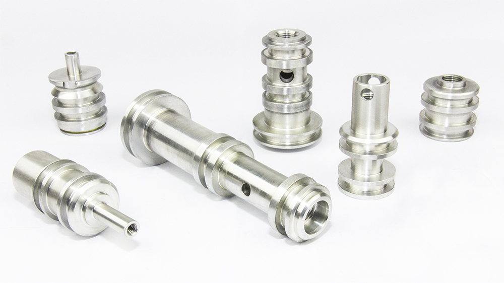
Electron Beam PVD Explained: High-Flux Nano-Finishing for Extreme Environments
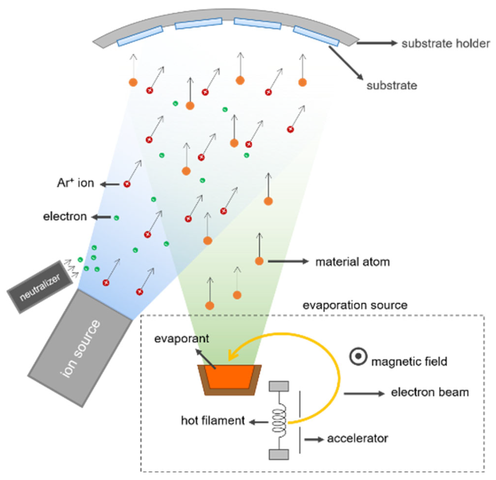
1. What Is Electron Beam PVD?
| Metric | Electron Beam PVD | Magnetron Sputter | Electroplated Ni |
|---|---|---|---|
| Thickness Range | 5 nm–5 µm | 1–5 µm | 5–50 µm |
| Deposition Rate | 5–50 µm/h | 0.5–2 µm/h | 5–20 µm/h |
| Hardness (HV) | 2 800–3 500 | 2 500–3 200 | 700 |
| Max Service Temp | 1 000 °C | 400 °C | 300 °C |
| REACH Status | ✅ Compliant | Compliant | ⚠️ Restricted |
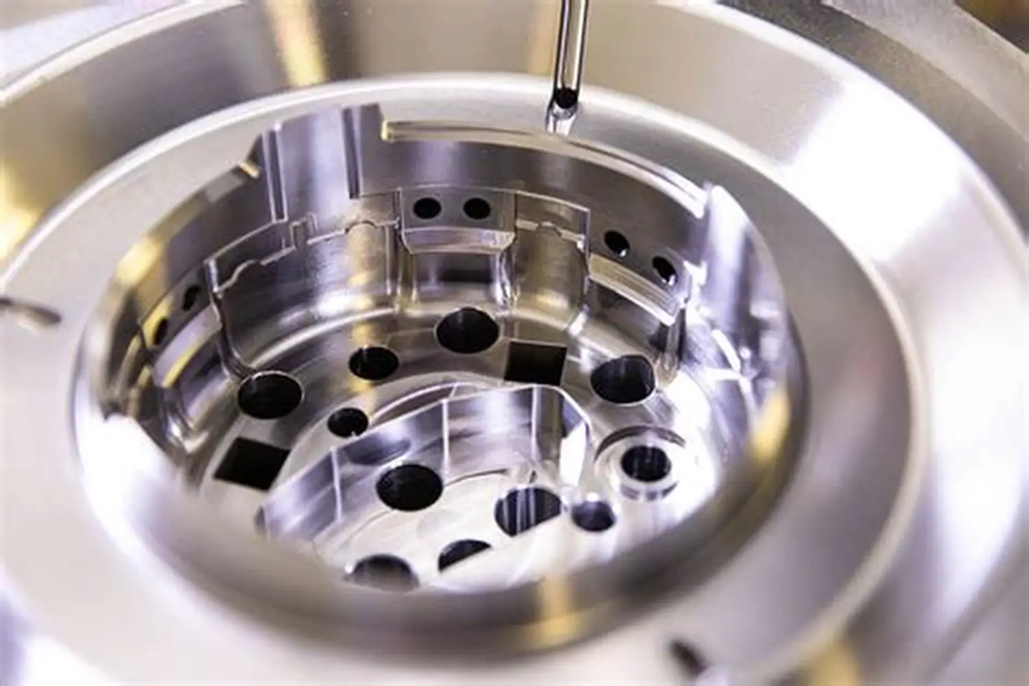
2. The 6-Step e-Beam Process – From Cathode to Coating
| Step | Vacuum Level | Temp (°C) | Action | KPI |
|---|---|---|---|---|
| 1 Plasma Clean | 10⁻³ mbar | 25 | Ar⁺ removes oxide & oil | Contact angle ≤ 8° |
| 2 Pre-heat | 10⁻³ mbar | 150–500 | Substrate heating | ΔT ≤ 5 °C |
| 3 E-Beam Ignition | 10⁻⁴ mbar | 1 500–2 500 | Tungsten filament → electron beam | Beam current 0.5–5 A |
| 4 Evaporation | 10⁻⁴ mbar | 1 500–2 500 | Solid ingot → vapor cloud | Evaporation rate 1–10 g/min |
| 5 Dense Film Growth | 10⁻⁴ mbar | 150–800 | Vapor condenses on substrate | ±3 nm uniformity |
| 6 QA & Pack | Air | 25 | CT + nano-indent + salt-spray | CpK ≥ 1.67 |
3. 2024 Performance Matrix – e-Beam vs Other PVD Routes
| Method | Thickness (µm) | Hardness (HV) | Salt-Spray (h) | Max Temp (°C) | Typical Use |
|---|---|---|---|---|---|
| Electroplated Ni | 25 | 700 | 48 | 300 | Decorative trim |
| Spray Paint | 50 | 200 | 48 | 150 | Body panels |
| Filtered Arc ta-C | 0.5 | 3 000 | 1 000 | 400 | Medical drills |
| HiPIMS Sputter | 1 | 3 200 | 1 200 | 1 000 | EV motor punches |
| Electron Beam PVD | 2 | 3 500 | 1 200 | 1 000 | Turbine blades |
4. Three 2024 Case Studies
Case 1 – Aerospace Turbine Blade
-
Client: European OEM, 2024
-
Problem: Fretting at 850 °C dovetail
-
e-Beam Stack: TiAlCrN 2 µm + a-C:H 200 nm
-
Outcome: Wear scar < 5 µm after 1 000 h; maintenance interval doubled
Case 2 – EV Motor Lamination Die
-
Client: US EV Tier-1, 2024
-
Problem: 0.35 mm electrical steel sticking at 400 °C
-
e-Beam Stack: CrAlON 1.8 µm + a-C:H 50 nm
-
Outcome: Tool life 4× longer, scrap −40 %
Case 3 – Medical Drill
-
Client: US MedTech startup, 2024
-
Problem: 316L needs low-friction piercing
-
e-Beam Stack: ta-C 300 nm + Cr 30 nm adhesion
-
Outcome: Penetration force −25 %, CE mark granted
5. Global Standards & Sustainability
-
ISO 9001:2015 / IATF 16949 / ISO 13485
-
REACH, RoHS, FDA 21 CFR §175.300
-
Energy: 0.35 kWh per m² (e-beam)
-
Waste: Zero liquid effluent
6. 7-Day Delivery Timeline
| Milestone | Lead Time |
|---|---|
| DFM + Quote | 24 h |
| Prototype (1–10 pcs) | 48 h |
| Validation (CT, salt-spray) | 5 days |
| Mass Production | 7–10 days |
| Door-to-Door Delivery | 12 days total |
7. FAQs – Which e-Beam Stack Fits My Job?
| Question | Answer |
|---|---|
| Can e-beam coat plastics? | Yes—metallised PEEK, LCP. |
| Largest part? | 800 mm Ø × 1200 mm L. |
| Minimum order? | 1 piece. |
8. How to Start Tomorrow
-
Email [email protected] with STEP/IGES.
-
Specify substrate, load, temperature, thickness budget.
-
Receive DFM + e-beam stack + quote within 48 h.
-
Approve → 3-day prototype → volume ramp.
Explore complementary services: Professional Anodizing Near Me
Ready to master electron beam PVD?
Contact JLY Precision Tech—the China expert who explains the process and delivers tomorrow.
Contact JLY Precision Tech—the China expert who explains the process and delivers tomorrow.