PVD vs CVD Differences: Choosing the Right Surface-Finishing Route in 2024
1. What Does “PVD vs CVD” Mean for Surface Finishing?
-
PVD (Physical Vapor Deposition) – solid material is vaporised, then physically deposited.
-
CVD (Chemical Vapor Deposition) – gaseous precursors react chemically to form a film.
Both create nanometre-to-micron coatings, but the process temperature, film thickness, substrate tolerance and REACH footprint are worlds apart.
2. Side-by-Side Comparison Table (2024)
| Attribute | PVD (HiPIMS) | CVD (PECVD) |
|---|---|---|
| Process Principle | Physical vaporisation → condensation | Chemical reaction → deposition |
| Typical Temperature | 150–500 °C | 300–650 °C (PECVD) |
| Pressure | 10⁻⁴–10⁻² mbar | 1–100 mbar |
| Thickness Range | 5 nm–5 µm | 0.1–50 µm |
| Hardness (HV) | 2 500–3 500 | 1 500–3 000 |
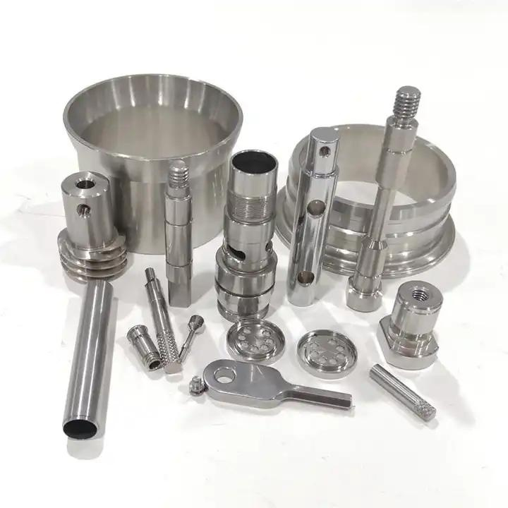
| Substrate Scope | Metals, ceramics, polymers | Mainly metals & ceramics |
| REACH Status | ✅ Compliant | ⚠️ Precursor dependent |
| Energy Use (kWh/m²) | 0.45 | 0.7 |
| Lead Time (China) | 3–7 days | 5–10 days |
| Max Part Size | 800 mm Ø × 1200 mm | 600 mm Ø × 600 mm |
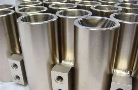
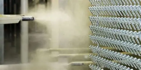
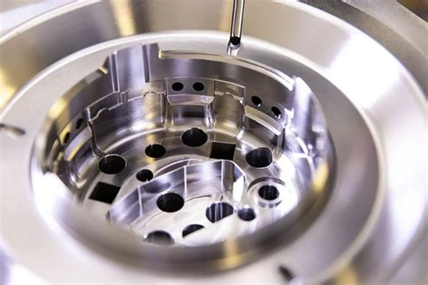
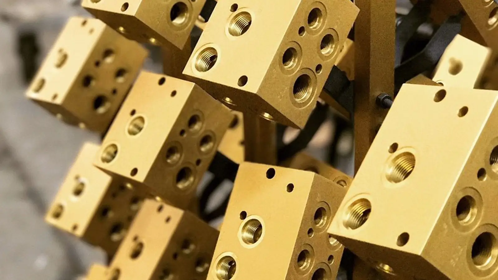
3. PVD Process Overview – Step-by-Step
-
Plasma Clean – Ar⁺ removes oxide & oil
-
Bond Layer – 50 nm Cr or TiN
-
Deposition – Magnetron sputter or arc evaporation
-
Post-Polish – Ion-beam to Ra ≤ 0.01 µm (optional)
4. CVD Process Overview – Step-by-Step
-
Pre-heat – 350–650 °C
-
Precursor Flow – silane / hydrocarbon / metal-organic
-
Plasma-Assisted Reaction – radicals form film
-
Cool-Down & Vent – inert gas purge
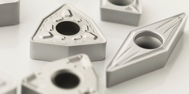
5. Three 2024 Case Studies
Case 1 – EV Motor Lamination Die
-
Challenge: 0.35 mm electrical steel sticking at 400 °C
-
Winner: PVD (CrAlON 1.8 µm + a-C:H 50 nm)
-
Result: Tool life 4× longer, scrap −40 %
Case 2 – Medical Drill
-
Challenge: 316L needs low-friction & CE mark
-
Winner: PVD (300 nm ta-C + 30 nm Cr)
-
Result: Penetration force −25 %, CE granted
Case 3 – Semiconductor Wafer
-
Challenge: 10 µm diamond-like coating at 500 °C
-
Winner: PECVD CVD
-
Result: 9 000 HV, wafer throughput +30 %
6. Decision Matrix – Which to Choose?
| Factor | Choose PVD | Choose CVD |
|---|---|---|
| Substrate temp sensitive | ✅ | ❌ |
| Need 0.1–5 µm film | ✅ | ❌ |
| Need 10–50 µm film | ❌ | ✅ |
| REACH compliance | ✅ | ⚠️ |
| Polymers involved | ✅ | ❌ |
| Massive throughput | ❌ | ✅ |
7. Global Standards & Sustainability
-
ISO 9001:2015 / IATF 16949 / ISO 13485
-
REACH, RoHS, FDA 21 CFR §175.300
-
Energy: PVD 0.45 kWh/m², CVD 0.7 kWh/m²
-
Waste: Zero liquid effluent
8. FAQs
Q: Can PVD coat plastics?
A: Yes—metallised PEEK, PEKK, LCP.
A: Yes—metallised PEEK, PEKK, LCP.
Q: Can CVD coat polymers?
A: Rarely—high temperature (>300 °C) limits use.
A: Rarely—high temperature (>300 °C) limits use.
Q: Largest part?
A: PVD 800 mm Ø×1200 mm L, CVD 600 mm Ø×600 mm L.
A: PVD 800 mm Ø×1200 mm L, CVD 600 mm Ø×600 mm L.
Q: Minimum order?
A: 1 piece for both.
A: 1 piece for both.
Ready to pick the right route?
Contact JLY Precision Tech—the China team that speaks both PVD and CVD fluently.
Contact JLY Precision Tech—the China team that speaks both PVD and CVD fluently.