
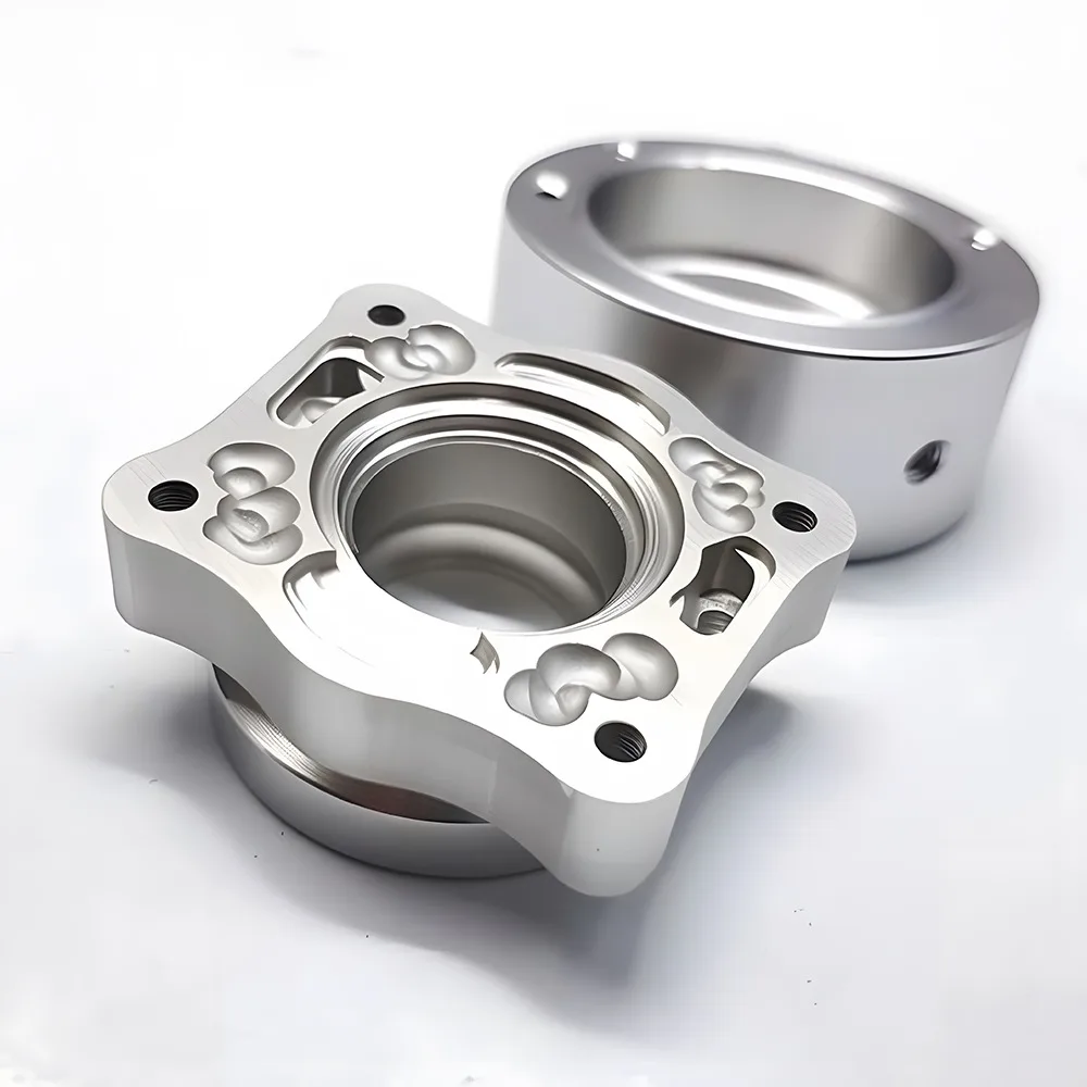
PVD Finish Meaning: Unveiling the Power of Physical Vapor Deposition in Surface Finishing
1. What Does PVD Finish Mean?
A PVD finish refers to the final surface treatment achieved through Physical Vapor Deposition, where solid materials are vaporized and deposited as thin films onto a substrate. This process results in surfaces that are harder, more durable, and chemically inert compared to traditional coatings like electroplated chrome or paint.
| Attribute | PVD Finish | Electroplated Ni | Spray Paint |
|---|---|---|---|
| Thickness | 5 nm–5 µm | 5–50 µm | 25–100 µm |
| Hardness (HV) | 2 500–3 500 | 700 | 200 |
| Max Temp (air) | 1 000 °C | 300 °C | 150 °C |
| REACH Status | Compliant | Restricted | Limited |
| Uniformity | ±5 nm | ±10 µm | ±25 µm |
2. The Science Behind PVD Finish
PVD involves several key steps, each meticulously controlled to ensure the highest quality finish:
| Step | Vacuum Level | Temperature | Action |
|---|---|---|---|
| Pre-clean | 10⁻³ mbar | 25 °C | Plasma etching removes contaminants |
| Bond Layer | 10⁻³ mbar | 200 °C | 50 nm Cr or TiN for adhesion |
| Deposition | 10⁻⁴ mbar | 150–500 °C | Vapor atoms condense to form film |
| Post-polish | Air | 25 °C | CMP or ion-beam finishing to Ra ≤ 0.01 µm |
The two look alike under a microscope and behave nothing alike in service. Choosing is discussed in PVD vs CVD coatings.
3. PVD Finish vs Traditional Surface Treatments – 2024 Comparison
| Method | Thickness (µm) | Hardness (HV) | Salt-Spray (h) | Max Temp (°C) | Typical Use |
|---|---|---|---|---|---|
| Electroplated Ni | 25 | 700 | 48 | 300 | Decorative trim |
| Spray Paint | 50 | 200 | 48 | 150 | Body panels |
| Traditional DLC | 2 | 2 000 | 500 | 400 | Cutting tools |
| HiPIMS TiAlCrN | 2 | 2 900 | 1 200 | 1 000 | Turbine blades |
| Filtered Arc ta-C | 0.5 | 3 000 | 1 000 | 400 | Medical drills |
| Reactive CrAlON | 1 | 2 400 | 800 | 600 | EV motor punches |
4. Real-World Applications and Case Studies
Case 1 – EV Motor Punch
-
Client: US EV Tier-1
-
Challenge: 0.35 mm electrical steel sticking at 400 °C
-
Solution: 1.8 µm CrAlON + 50 nm a-C:H
-
Result: Tool life 4× longer, scrap −40 %
Case 2 – Medical Staple
-
Client: US MedTech startup
-
Challenge: Low-friction 316L piercing
-
Solution: 300 nm ta-C + 30 nm Cr adhesion
-
Result: Penetration force −25 %, CE mark granted
Case 3 – Smartphone EMI Shield
-
Client: Global mobile OEM
-
Challenge: 6 GHz EMI leakage in SiC inverter
-
Solution: 150 nm Ag/Ni/Cr multilayer
-
Result: Shielding 85 dB @ 6 GHz, CISPR 25 passed
5. Step-by-Step PVD Process
| Stage | Actions | KPIs | Lead Time |
|---|---|---|---|
| 1 | Design Review | CAD + CFD + DOE | 24 h |
| 2 | Prototype | 1–10 pcs | 48 h |
| 3 | Validation | CT, CMM, salt-spray | 5 days |
| 4 | Scale-Up | SPC, poka-yoke | 2 days |
| 5 | Production | 24/7 lights-out | 7–10 days |
| 6 | QA | Calot, CpK ≥1.67 | 12 h |
6. Global Standards and Sustainability
-
ISO 9001:2015 / IATF 16949 / ISO 13485
-
REACH, RoHS, FDA 21 CFR §175.300
-
Energy: 0.45 kWh per m²
-
Waste: Zero liquid effluent
7. FAQs About PVD Finish
Q: What substrates can PVD coat? A: Steel, stainless, titanium, aluminum, ceramics, plastics.
Q: Largest part? A: 800 mm Ø × 1200 mm L.
Q: Minimum order quantity? A: 1 piece.
8. How to Get Started with PVD Finish
-
Email [email protected] with STEP/IGES files.
-
Specify substrate, load, temperature, thickness budget.
-
Receive DFM + coating stack + quotation within 48 h.
-
No MOQ; volume discounts from 100 pcs.
Explore complementary services: Professional Anodizing Near Me
Related Reading
If you want to go deeper into the specifics, these pages cover the adjacent details:
- China PVD Coating Service
- PVD Coating Durability Guide
- PVD Coating Service for Precision Machined Parts
A finished sample settles arguments about the substrate tempering temperature faster than a spec sheet does. Ask for one through the JLYPT quote page; the PVD coating service shows what the surface looks like off the line.